DATA SHEET - IEETA
DATA SHEET - IEETA
DATA SHEET - IEETA

You also want an ePaper? Increase the reach of your titles
YUMPU automatically turns print PDFs into web optimized ePapers that Google loves.
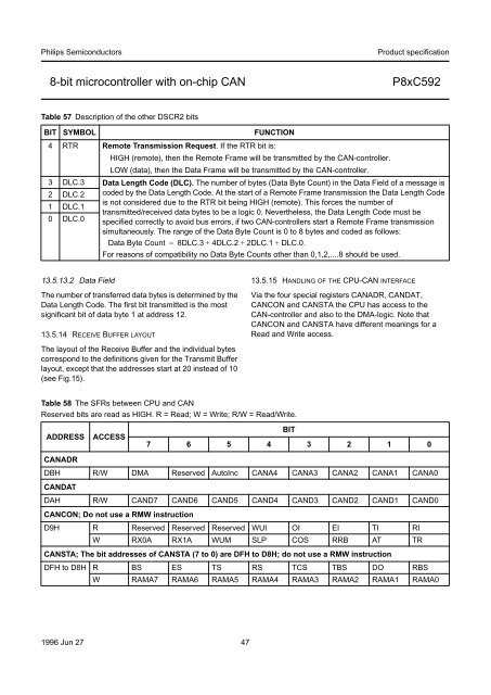
Philips Semiconductors Product specification<br />
8-bit microcontroller with on-chip CAN P8xC592<br />
Table 57 Description of the other DSCR2 bits<br />
BIT SYMBOL FUNCTION<br />
4 RTR Remote Transmission Request. If the RTR bit is:<br />
HIGH (remote), then the Remote Frame will be transmitted by the CAN-controller.<br />
LOW (data), then the Data Frame will be transmitted by the CAN-controller.<br />
3 DLC.3 Data Length Code (DLC). The number of bytes (Data Byte Count) in the Data Field of a message is<br />
2 DLC.2 coded by the Data Length Code. At the start of a Remote Frame transmission the Data Length Code<br />
1<br />
0<br />
DLC.1<br />
DLC.0<br />
is not considered due to the RTR bit being HIGH (remote). This forces the number of<br />
transmitted/received data bytes to be a logic 0. Nevertheless, the Data Length Code must be<br />
specified correctly to avoid bus errors, if two CAN-controllers start a Remote Frame transmission<br />
simultaneously. The range of the Data Byte Count is 0 to 8 bytes and coded as follows:<br />
Data Byte Count = 8DLC.3 + 4DLC.2 + 2DLC.1 + DLC.0.<br />
For reasons of compatibility no Data Byte Counts other than 0,1,2,....8 should be used.<br />
13.5.13.2 Data Field<br />
The number of transferred data bytes is determined by the<br />
Data Length Code. The first bit transmitted is the most<br />
significant bit of data byte 1 at address 12.<br />
13.5.14 RECEIVE BUFFER LAYOUT<br />
The layout of the Receive Buffer and the individual bytes<br />
correspond to the definitions given for the Transmit Buffer<br />
layout, except that the addresses start at 20 instead of 10<br />
(see Fig.15).<br />
Table 58 The SFRs between CPU and CAN<br />
Reserved bits are read as HIGH. R = Read; W = Write; R/W = Read/Write.<br />
ADDRESS ACCESS<br />
1996 Jun 27 47<br />
13.5.15 HANDLING OF THE CPU-CAN INTERFACE<br />
Via the four special registers CANADR, CANDAT,<br />
CANCON and CANSTA the CPU has access to the<br />
CAN-controller and also to the DMA-logic. Note that<br />
CANCON and CANSTA have different meanings for a<br />
Read and Write access.<br />
BIT<br />
7 6 5 4 3 2 1 0<br />
CANADR<br />
DBH<br />
CANDAT<br />
R/W DMA Reserved AutoInc CANA4 CANA3 CANA2 CANA1 CANA0<br />
DAH R/W CAND7 CAND6 CAND5 CAND4 CAND3 CAND2 CAND1 CAND0<br />
CANCON; Do not use a RMW instruction<br />
D9H R Reserved Reserved Reserved WUI OI EI TI RI<br />
W RX0A RX1A WUM SLP COS RRB AT TR<br />
CANSTA; The bit addresses of CANSTA (7 to 0) are DFH to D8H; do not use a RMW instruction<br />
DFH to D8H R BS ES TS RS TCS TBS DO RBS<br />
W RAMA7 RAMA6 RAMA5 RAMA4 RAMA3 RAMA2 RAMA1 RAMA0