DATA SHEET - IEETA
DATA SHEET - IEETA
DATA SHEET - IEETA

You also want an ePaper? Increase the reach of your titles
YUMPU automatically turns print PDFs into web optimized ePapers that Google loves.
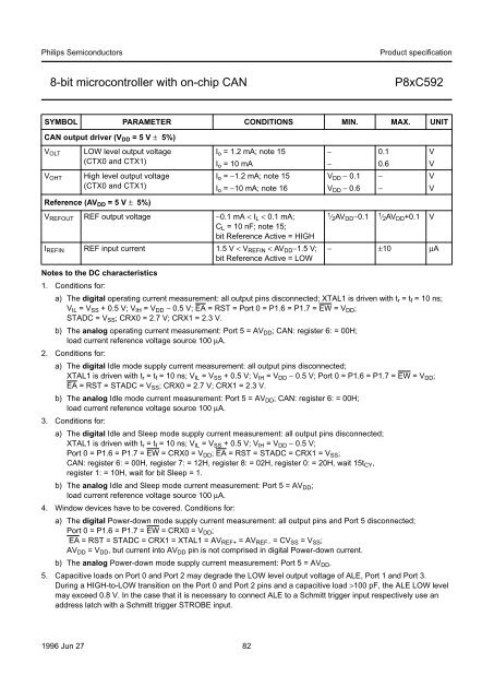
Philips Semiconductors Product specification<br />
8-bit microcontroller with on-chip CAN P8xC592<br />
SYMBOL PARAMETER CONDITIONS MIN. MAX. UNIT<br />
CAN output driver (VDD =5V± 5%)<br />
VOLT LOW level output voltage<br />
(CTX0 and CTX1)<br />
VOHT<br />
High level output voltage<br />
(CTX0 and CTX1)<br />
Reference (AVDD =5V± 5%)<br />
VREFOUT REF output voltage −0.1 mA < IL < 0.1 mA;<br />
CL = 10 nF; note 15;<br />
bit Reference Active = HIGH<br />
IREFIN REF input current 1.5 V < VREFIN < AVDD−1.5 V;<br />
bit Reference Active = LOW<br />
Notes to the DC characteristics<br />
1. Conditions for:<br />
a) The digital operating current measurement: all output pins disconnected; XTAL1 is driven with tr =tf= 10 ns;<br />
VIL =VSS + 0.5 V; VIH =VDD − 0.5 V; EA = RST = Port 0 = P1.6 = P1.7 = EW = VDD;<br />
STADC = VSS; CRX0 = 2.7 V; CRX1 = 2.3 V.<br />
b) The analog operating current measurement: Port 5 = AVDD; CAN: register 6: = 00H;<br />
load current reference voltage source 100 μA.<br />
2. Conditions for:<br />
a) The digital Idle mode supply current measurement: all output pins disconnected;<br />
XTAL1 is driven with tr =tf= 10 ns; VIL =VSS + 0.5 V; VIH =VDD − 0.5 V; Port 0 = P1.6 = P1.7 = EW=VDD;<br />
EA = RST = STADC = VSS; CRX0 = 2.7 V; CRX1 = 2.3 V.<br />
b) The analog Idle mode current measurement: Port 5 = AVDD; CAN: register 6: = 00H;<br />
load current reference voltage source 100 μA.<br />
3. Conditions for:<br />
a) The digital Idle and Sleep mode supply current measurement: all output pins disconnected;<br />
XTAL1 is driven with tr =tf= 10 ns; VIL =VSS + 0.5 V; VIH =VDD − 0.5 V;<br />
Port 0 = P1.6 = P1.7 = EW = CRX0 = VDD; EA = RST = STADC = CRX1 = VSS;<br />
CAN: register 6: = 00H, register 7: = 12H, register 8: = 02H, register 0: = 20H, wait 15tCY,<br />
register 1: = 10H, wait for bit Sleep = 1.<br />
b) The analog Idle and Sleep mode current measurement: Port 5=AVDD;<br />
load current reference voltage source 100 μA.<br />
4. Window devices have to be covered. Conditions for:<br />
a) The digital Power-down mode supply current measurement: all output pins and Port 5 disconnected;<br />
Port 0 = P1.6 = P1.7 = EW = CRX0 = VDD;<br />
EA = RST = STADC = CRX1 = XTAL1 = AVREF+ = AVREF− = CVSS =VSS;<br />
AVDD =VDD, but current into AVDD pin is not comprised in digital Power-down current.<br />
b) The analog Power-down mode supply current measurement: Port 5 = AVDD.<br />
5. Capacitive loads on Port 0 and Port 2 may degrade the LOW level output voltage of ALE, Port 1 and Port 3.<br />
During a HIGH-to-LOW transition on the Port 0 and Port 2 pins and a capacitive load >100 pF, the ALE LOW level<br />
may exceed 0.8 V. In the case that it is necessary to connect ALE to a Schmitt trigger input respectively use an<br />
address latch with a Schmitt trigger STROBE input.<br />
1996 Jun 27 82<br />
Io = 1.2 mA; note 15 − 0.1 V<br />
Io =10mA − 0.6 V<br />
Io = −1.2 mA; note 15 VDD − 0.1 − V<br />
Io = −10 mA; note 16 VDD − 0.6 − V<br />
1 ⁄2AVDD−0.1 1 ⁄2AVDD+0.1 V<br />
− ±10 μA