

PIC16F8X, 18-Pin FLASH/EEPROM 8-Bit MCU Data Sheet - Microchip
PIC16F8X, 18-Pin FLASH/EEPROM 8-Bit MCU Data Sheet - Microchip
PIC16F8X, 18-Pin FLASH/EEPROM 8-Bit MCU Data Sheet - Microchip

You also want an ePaper? Increase the reach of your titles
YUMPU automatically turns print PDFs into web optimized ePapers that Google loves.
Devices Included in this <strong>Data</strong> <strong>Sheet</strong>:<br />
• PIC16F83<br />
• PIC16F84<br />
• PIC16CR83<br />
• PIC16CR84<br />
• Extended voltage range devices available<br />
(PIC16LF8X, PIC16LCR8X)<br />
High Performance RISC CPU Features:<br />
• Only 35 single word instructions to learn<br />
• All instructions single cycle except for program<br />
branches which are two-cycle<br />
• Operating speed: DC - 10 MHz clock input<br />
DC - 400 ns instruction cycle<br />
Device<br />
Program<br />
Memory<br />
(words)<br />
<strong>Data</strong><br />
RAM<br />
(bytes)<br />
<strong>Data</strong><br />
<strong>EEPROM</strong><br />
(bytes)<br />
Max.<br />
Freq<br />
(MHz)<br />
PIC16F83 512 Flash 36 64 10<br />
PIC16F84 1 K Flash 68 64 10<br />
PIC16CR83 512 ROM 36 64 10<br />
PIC16CR84 1 K ROM 68 64 10<br />
• 14-bit wide instructions<br />
• 8-bit wide data path<br />
• 15 special function hardware registers<br />
• Eight-level deep hardware stack<br />
• Direct, indirect and relative addressing modes<br />
• Four interrupt sources:<br />
- External RB0/INT pin<br />
- TMR0 timer overflow<br />
- PORTB interrupt on change<br />
- <strong>Data</strong> <strong>EEPROM</strong> write complete<br />
• 1000 erase/write cycles Flash program memory<br />
• 10,000,000 erase/write cycles <strong>EEPROM</strong> data memory<br />
• <strong>EEPROM</strong> <strong>Data</strong> Retention > 40 years<br />
Peripheral Features:<br />
• 13 I/O pins with individual direction control<br />
• High current sink/source for direct LED drive<br />
- 25 mA sink max. per pin<br />
- 20 mA source max. per pin<br />
• TMR0: 8-bit timer/counter with 8-bit<br />
programmable prescaler<br />
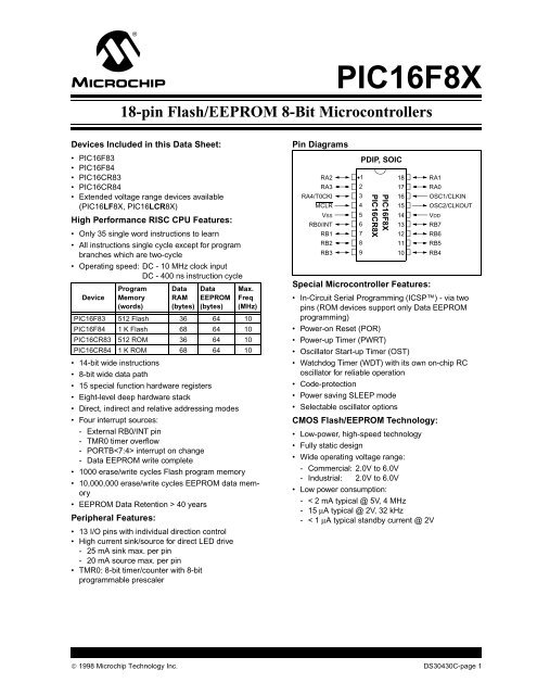
<strong>Pin</strong> Diagrams<br />
RA2<br />
RA3<br />
RA4/T0CKI<br />
MCLR<br />
VSS<br />
RB0/INT<br />
RB1<br />
RB2<br />
RB3<br />
<strong>PIC16F8X</strong><br />
<strong>18</strong>-pin Flash/<strong>EEPROM</strong> 8-<strong>Bit</strong> Microcontrollers<br />
Special Microcontroller Features:<br />
RA1<br />
RA0<br />
OSC1/CLKIN<br />
OSC2/CLKOUT<br />
VDD<br />
RB7<br />
RB6<br />
RB5<br />
RB4<br />
• In-Circuit Serial Programming (ICSP) - via two<br />
pins (ROM devices support only <strong>Data</strong> <strong>EEPROM</strong><br />
programming)<br />
• Power-on Reset (POR)<br />
• Power-up Timer (PWRT)<br />
• Oscillator Start-up Timer (OST)<br />
• Watchdog Timer (WDT) with its own on-chip RC<br />
oscillator for reliable operation<br />
• Code-protection<br />
• Power saving SLEEP mode<br />
• Selectable oscillator options<br />
CMOS Flash/<strong>EEPROM</strong> Technology:<br />
• Low-power, high-speed technology<br />
• Fully static design<br />
• Wide operating voltage range:<br />
- Commercial: 2.0V to 6.0V<br />
- Industrial: 2.0V to 6.0V<br />
• Low power consumption:<br />
- < 2 mA typical @ 5V, 4 MHz<br />
- 15 μA typical @ 2V, 32 kHz<br />
- < 1 μA typical standby current @ 2V<br />
© 1998 <strong>Microchip</strong> Technology Inc. DS30430C-page 1<br />
•1<br />
2<br />
3<br />
4<br />
5<br />
6<br />
7<br />
8<br />
9<br />
PDIP, SOIC<br />
<strong>PIC16F8X</strong><br />
PIC16CR8X<br />
<strong>18</strong><br />
17<br />
16<br />
15<br />
14<br />
13<br />
12<br />
11<br />
10
<strong>PIC16F8X</strong><br />
Table of Contents<br />
1.0 General Description ...................................................................................................................................................................... 3<br />
2.0 <strong>PIC16F8X</strong> Device Varieties .......................................................................................................................................................... 5<br />
3.0 Architectural Overview.................................................................................................................................................................. 7<br />
4.0 Memory Organization ................................................................................................................................................................. 11<br />
5.0 I/O Ports...................................................................................................................................................................................... 21<br />
6.0 Timer0 Module and TMR0 Register............................................................................................................................................ 27<br />
7.0 <strong>Data</strong> <strong>EEPROM</strong> Memory.............................................................................................................................................................. 33<br />
8.0 Special Features of the CPU ...................................................................................................................................................... 37<br />
9.0 Instruction Set Summary ............................................................................................................................................................ 53<br />
10.0 Development Support ................................................................................................................................................................. 69<br />
11.0 Electrical Characteristics for PIC16F83 and PIC16F84.............................................................................................................. 73<br />
12.0 Electrical Characteristics for PIC16CR83 and PIC16CR84........................................................................................................ 85<br />
13.0 DC & AC Characteristics Graphs/Tables.................................................................................................................................... 97<br />
14.0 Packaging Information .............................................................................................................................................................. 109<br />
Appendix A: Feature Improvements - From PIC16C5X To <strong>PIC16F8X</strong> .......................................................................................... 113<br />
Appendix B: Code Compatibility - from PIC16C5X to <strong>PIC16F8X</strong>.................................................................................................. 113<br />
Appendix C: What’s New In This <strong>Data</strong> <strong>Sheet</strong>................................................................................................................................. 114<br />
Appendix D: What’s Changed In This <strong>Data</strong> <strong>Sheet</strong> ......................................................................................................................... 114<br />
Appendix E: Conversion Considerations - PIC16C84 to PIC16F83/F84 And PIC16CR83/CR84.................................................. 115<br />
Index ................................................................................................................................................................................................. 117<br />
On-Line Support................................................................................................................................................................................. 119<br />
Reader Response .............................................................................................................................................................................. 120<br />
<strong>PIC16F8X</strong> Product Identification System ........................................................................................................................................... 121<br />
Sales and Support.............................................................................................................................................................................. 121<br />
To Our Valued Customers<br />
We constantly strive to improve the quality of all our products and documentation. We have spent a great deal of<br />
time to ensure that these documents are correct. However, we realize that we may have missed a few things. If you<br />
find any information that is missing or appears in error, please use the reader response form in the back of this data<br />
sheet to inform us. We appreciate your assistance in making this a better document.<br />
DS30430C-page 2 © 1998 <strong>Microchip</strong> Technology Inc.
1.0 GENERAL DESCRIPTION<br />
The <strong>PIC16F8X</strong> is a group in the PIC16CXX family of<br />
low-cost, high-performance, CMOS, fully-static, 8-bit<br />
microcontrollers. This group contains the following<br />
devices:<br />
• PIC16F83<br />
• PIC16F84<br />
• PIC16CR83<br />
• PIC16CR84<br />
All PICmicro microcontrollers employ an advanced<br />
RISC architecture. <strong>PIC16F8X</strong> devices have enhanced<br />
core features, eight-level deep stack, and multiple<br />
internal and external interrupt sources. The separate<br />
instruction and data buses of the Harvard architecture<br />
allow a 14-bit wide instruction word with a separate<br />
8-bit wide data bus. The two stage instruction pipeline<br />
allows all instructions to execute in a single cycle,<br />
except for program branches (which require two<br />
cycles). A total of 35 instructions (reduced instruction<br />
set) are available. Additionally, a large register set is<br />
used to achieve a very high performance level.<br />
<strong>PIC16F8X</strong> microcontrollers typically achieve a 2:1 code<br />
compression and up to a 4:1 speed improvement (at 20<br />
MHz) over other 8-bit microcontrollers in their class.<br />
The <strong>PIC16F8X</strong> has up to 68 bytes of RAM, 64 bytes of<br />
<strong>Data</strong> <strong>EEPROM</strong> memory, and 13 I/O pins. A timer/<br />
counter is also available.<br />
The PIC16CXX family has special features to reduce<br />
external components, thus reducing cost, enhancing<br />
system reliability and reducing power consumption.<br />
There are four oscillator options, of which the single pin<br />
RC oscillator provides a low-cost solution, the LP<br />
oscillator minimizes power consumption, XT is a<br />
standard crystal, and the HS is for High Speed crystals.<br />
The SLEEP (power-down) mode offers power saving.<br />
The user can wake the chip from sleep through several<br />
external and internal interrupts and resets.<br />
A highly reliable Watchdog Timer with its own on-chip<br />
RC oscillator provides protection against software lockup.<br />
The devices with Flash program memory allow the<br />
same device package to be used for prototyping and<br />
production. In-circuit reprogrammability allows the<br />
code to be updated without the device being removed<br />
from the end application. This is useful in the<br />
development of many applications where the device<br />
may not be easily accessible, but the prototypes may<br />
require code updates. This is also useful for remote<br />
applications where the code may need to be updated<br />
(such as rate information).<br />
<strong>PIC16F8X</strong><br />
Table 1-1 lists the features of the <strong>PIC16F8X</strong>. A simplified<br />
block diagram of the <strong>PIC16F8X</strong> is shown in<br />
Figure 3-1.<br />
The <strong>PIC16F8X</strong> fits perfectly in applications ranging<br />
from high speed automotive and appliance motor<br />
control to low-power remote sensors, electronic locks,<br />
security devices and smart cards. The Flash/<strong>EEPROM</strong><br />
technology makes customization of application<br />
programs (transmitter codes, motor speeds, receiver<br />
frequencies, security codes, etc.) extremely fast and<br />
convenient. The small footprint packages make this<br />
microcontroller series perfect for all applications with<br />
space limitations. Low-cost, low-power, high<br />
performance, ease-of-use and I/O flexibility make the<br />
<strong>PIC16F8X</strong> very versatile even in areas where no<br />
microcontroller use has been considered before<br />
(e.g., timer functions; serial communication; capture,<br />
compare and PWM functions; and co-processor<br />
applications).<br />
The serial in-system programming feature (via two<br />
pins) offers flexibility of customizing the product after<br />
complete assembly and testing. This feature can be<br />
used to serialize a product, store calibration data, or<br />
program the device with the current firmware before<br />
shipping.<br />
1.1 Family and Upward Compatibility<br />
Those users familiar with the PIC16C5X family of<br />
microcontrollers will realize that this is an enhanced<br />
version of the PIC16C5X architecture. Please refer to<br />
Appendix A for a detailed list of enhancements. Code<br />
written for PIC16C5X devices can be easily ported to<br />
<strong>PIC16F8X</strong> devices (Appendix B).<br />
1.2 Development Support<br />
The PIC16CXX family is supported by a full-featured<br />
macro assembler, a software simulator, an in-circuit<br />
emulator, a low-cost development programmer and a<br />
full-featured programmer. A “C” compiler and fuzzy<br />
logic support tools are also available.<br />
© 1998 <strong>Microchip</strong> Technology Inc. DS30430C-page 3
<strong>PIC16F8X</strong><br />
TABLE 1-1 <strong>PIC16F8X</strong> FAMILY OF DEVICES<br />
PIC16F83 PIC16CR83 PIC16F84 PIC16CR84<br />
Clock<br />
Maximum Frequency<br />
of Operation (MHz)<br />
10 10 10 10<br />
Flash Program Memory 512 — 1K —<br />
<strong>EEPROM</strong> Program Memory — — — —<br />
Memory ROM Program Memory — 512 — 1K<br />
<strong>Data</strong> Memory (bytes) 36 36 68 68<br />
<strong>Data</strong> <strong>EEPROM</strong> (bytes) 64 64 64 64<br />
Peripherals Timer Module(s) TMR0 TMR0 TMR0 TMR0<br />
Interrupt Sources 4 4 4 4<br />
I/O <strong>Pin</strong>s 13 13 13 13<br />
Features Voltage Range (Volts) 2.0-6.0 2.0-6.0 2.0-6.0 2.0-6.0<br />
Packages <strong>18</strong>-pin DIP, <strong>18</strong>-pin DIP, <strong>18</strong>-pin DIP, <strong>18</strong>-pin DIP,<br />
SOIC<br />
SOIC<br />
SOIC<br />
SOIC<br />
All PICmicro Family devices have Power-on Reset, selectable Watchdog Timer, selectable code protect and high I/O current capability.<br />
All <strong>PIC16F8X</strong> Family devices use serial programming with clock pin RB6 and data pin RB7.<br />
DS30430C-page 4 © 1998 <strong>Microchip</strong> Technology Inc.
2.0 <strong>PIC16F8X</strong> DEVICE VARIETIES<br />
A variety of frequency ranges and packaging options<br />
are available. Depending on application and production<br />
requirements the proper device option can be selected<br />
using the information in this section. When placing<br />
orders, please use the “<strong>PIC16F8X</strong> Product<br />
Identification System” at the back of this data sheet to<br />
specify the correct part number.<br />
There are four device “types” as indicated in the device<br />
number.<br />
1. F, as in PIC16F84. These devices have Flash<br />
program memory and operate over the standard<br />
voltage range.<br />
2. LF, as in PIC16LF84. These devices have Flash<br />
program memory and operate over an extended<br />
voltage range.<br />
3. CR, as in PIC16CR83. These devices have<br />
ROM program memory and operate over the<br />
standard voltage range.<br />
4. LCR, as in PIC16LCR84. These devices have<br />
ROM program memory and operate over an<br />
extended voltage range.<br />
When discussing memory maps and other architectural<br />
features, the use of F and CR also implies the LF and<br />
LCR versions.<br />
2.1 Flash Devices<br />
These devices are offered in the lower cost plastic<br />
package, even though the device can be erased and<br />
reprogrammed. This allows the same device to be used<br />
for prototype development and pilot programs as well<br />
as production.<br />
A further advantage of the electrically-erasable Flash<br />
version is that it can be erased and reprogrammed incircuit,<br />
or by device programmers, such as <strong>Microchip</strong>'s<br />
PICSTART ® Plus or PRO MATE ® II programmers.<br />
2.2 Quick-Turnaround-Production (QTP)<br />
Devices<br />
<strong>Microchip</strong> offers a QTP Programming Service for<br />
factory production orders. This service is made<br />
available for users who choose not to program a<br />
medium to high quantity of units and whose code<br />
patterns have stabilized. The devices have all Flash<br />
locations and configuration options already programmed<br />
by the factory. Certain code and prototype<br />
verification procedures do apply before production<br />
shipments are available.<br />
For information on submitting a QTP code, please<br />
contact your <strong>Microchip</strong> Regional Sales Office.<br />
<strong>PIC16F8X</strong><br />
2.3 Serialized Quick-Turnaround-<br />
SM<br />
Production (SQTP ) Devices<br />
<strong>Microchip</strong> offers the unique programming service<br />
where a few user-defined locations in each device are<br />
programmed with different serial numbers. The serial<br />
numbers may be random, pseudo-random<br />
or sequential.<br />
Serial programming allows each device to have a<br />
unique number which can serve as an entry-code,<br />
password or ID number.<br />
For information on submitting a SQTP code, please<br />
contact your <strong>Microchip</strong> Regional Sales Office.<br />
2.4 ROM Devices<br />
Some of <strong>Microchip</strong>’s devices have a corresponding<br />
device where the program memory is a ROM. These<br />
devices give a cost savings over <strong>Microchip</strong>’s traditional<br />
user programmed devices (EPROM, <strong>EEPROM</strong>).<br />
ROM devices (PIC16CR8X) do not allow serialization<br />
information in the program memory space. The user<br />
may program this information into the <strong>Data</strong> <strong>EEPROM</strong>.<br />
For information on submitting a ROM code, please<br />
contact your <strong>Microchip</strong> Regional Sales Office.<br />
© 1998 <strong>Microchip</strong> Technology Inc. DS30430C-page 5
<strong>PIC16F8X</strong><br />
NOTES:<br />
DS30430C-page 6 © 1998 <strong>Microchip</strong> Technology Inc.
3.0 ARCHITECTURAL OVERVIEW<br />
The high performance of the PIC16CXX family can be<br />
attributed to a number of architectural features<br />
commonly found in RISC microprocessors. To begin<br />
with, the PIC16CXX uses a Harvard architecture. This<br />
architecture has the program and data accessed from<br />
separate memories. So the device has a program<br />
memory bus and a data memory bus. This improves<br />
bandwidth over traditional von Neumann architecture<br />
where program and data are fetched from the same<br />
memory (accesses over the same bus). Separating<br />
program and data memory further allows instructions to<br />
be sized differently than the 8-bit wide data word.<br />
PIC16CXX opcodes are 14-bits wide, enabling single<br />
word instructions. The full 14-bit wide program memory<br />
bus fetches a 14-bit instruction in a single cycle. A twostage<br />
pipeline overlaps fetch and execution of instructions<br />
(Example 3-1). Consequently, all instructions execute<br />
in a single cycle except for program branches.<br />
The PIC16F83 and PIC16CR83 address 512 x 14 of<br />
program memory, and the PIC16F84 and PIC16CR84<br />
address 1K x 14 program memory. All program memory<br />
is internal.<br />
The PIC16CXX can directly or indirectly address its<br />
register files or data memory. All special function<br />
registers including the program counter are mapped in<br />
the data memory. An orthogonal (symmetrical)<br />
instruction set makes it possible to carry out any operation<br />
on any register using any addressing mode. This<br />
symmetrical nature and lack of ‘special optimal<br />
situations’ make programming with the PIC16CXX<br />
simple yet efficient. In addition, the learning curve is<br />
reduced significantly.<br />
<strong>PIC16F8X</strong><br />
© 1998 <strong>Microchip</strong> Technology Inc. DS30430C-page 7
<strong>PIC16F8X</strong><br />
PIC16CXX devices contain an 8-bit ALU and working<br />
register. The ALU is a general purpose arithmetic unit.<br />
It performs arithmetic and Boolean functions between<br />
data in the working register and any register file.<br />
The ALU is 8-bits wide and capable of addition,<br />
subtraction, shift and logical operations. Unless<br />
otherwise mentioned, arithmetic operations are two’s<br />
complement in nature. In two-operand instructions,<br />
typically one operand is the working register<br />
(W register), and the other operand is a file register or<br />
an immediate constant. In single operand instructions,<br />
the operand is either the W register or a file register.<br />
FIGURE 3-1: <strong>PIC16F8X</strong> BLOCK DIAGRAM<br />
Flash/ROM<br />
Program<br />
Memory<br />
PIC16F83/CR83<br />
512 x 14<br />
PIC16F84/CR84<br />
1K x 14<br />
Program<br />
Bus<br />
14<br />
Instruction reg<br />
Instruction<br />
Decode &<br />
Control<br />
Timing<br />
Generation<br />
OSC2/CLKOUT<br />
OSC1/CLKIN<br />
13<br />
5<br />
Program Counter<br />
8 Level Stack<br />
(13-bit)<br />
Direct Addr<br />
8<br />
Power-up<br />
Timer<br />
Oscillator<br />
Start-up Timer<br />
Power-on<br />
Reset<br />
Watchdog<br />
Timer<br />
MCLR VDD, VSS<br />
The W register is an 8-bit working register used for ALU<br />
operations. It is not an addressable register.<br />
Depending on the instruction executed, the ALU may<br />
affect the values of the Carry (C), Digit Carry (DC), and<br />
Zero (Z) bits in the STATUS register. The C and DC bits<br />
operate as a borrow and digit borrow out bit,<br />
respectively, in subtraction. See the SUBLW and SUBWF<br />
instructions for examples.<br />
A simplified block diagram for the <strong>PIC16F8X</strong> is shown<br />
in Figure 3-1, its corresponding pin description is<br />
shown in Table 3-1.<br />
<strong>Data</strong> Bus<br />
RAM<br />
File Registers<br />
PIC16F83/CR83<br />
36 x 8<br />
PIC16F84/CR84<br />
68 x 8<br />
DS30430C-page 8 © 1998 <strong>Microchip</strong> Technology Inc.<br />
7<br />
Addr Mux<br />
ALU<br />
W reg<br />
7<br />
RAM Addr<br />
FSR reg<br />
STATUS reg<br />
MUX<br />
8<br />
Indirect<br />
Addr<br />
8<br />
<strong>EEPROM</strong> <strong>Data</strong> Memory<br />
EEDATA<br />
TMR0<br />
I/O Ports<br />
<strong>EEPROM</strong><br />
<strong>Data</strong> Memory<br />
64 x 8<br />
EEADR<br />
RA4/T0CKI<br />
RA3:RA0<br />
RB7:RB1<br />
RB0/INT
TABLE 3-1 <strong>PIC16F8X</strong> PINOUT DESCRIPTION<br />
<strong>Pin</strong> Name<br />
DIP<br />
No.<br />
SOIC<br />
No.<br />
I/O/P<br />
Type<br />
Buffer<br />
Type<br />
Description<br />
<strong>PIC16F8X</strong><br />
OSC1/CLKIN 16 16 I ST/CMOS (3) Oscillator crystal input/external clock source input.<br />
OSC2/CLKOUT 15 15 O — Oscillator crystal output. Connects to crystal or resonator in crystal<br />
oscillator mode. In RC mode, OSC2 pin outputs CLKOUT which has<br />
1/4 the frequency of OSC1, and denotes the instruction cycle rate.<br />
MCLR 4 4 I/P ST Master clear (reset) input/programming voltage input. This pin is an<br />
active low reset to the device.<br />
PORTA is a bi-directional I/O port.<br />
RA0 17 17 I/O TTL<br />
RA1 <strong>18</strong> <strong>18</strong> I/O TTL<br />
RA2 1 1 I/O TTL<br />
RA3 2 2 I/O TTL<br />
RA4/T0CKI 3 3 I/O ST Can also be selected to be the clock input to the TMR0 timer/<br />
counter. Output is open drain type.<br />
PORTB is a bi-directional I/O port. PORTB can be software programmed<br />
for internal weak pull-up on all inputs.<br />
RB0/INT 6 6 I/O TTL/ST (1)<br />
RB0/INT can also be selected as an external interrupt pin.<br />
RB1 7 7 I/O TTL<br />
RB2 8 8 I/O TTL<br />
RB3 9 9 I/O TTL<br />
RB4 10 10 I/O TTL Interrupt on change pin.<br />
RB5 11 11 I/O TTL Interrupt on change pin.<br />
RB6 12 12 I/O TTL/ST (2)<br />
Interrupt on change pin. Serial programming clock.<br />
RB7 13 13 I/O TTL/ST (2) Interrupt on change pin. Serial programming data.<br />
VSS 5 5 P — Ground reference for logic and I/O pins.<br />
VDD 14 14 P — Positive supply for logic and I/O pins.<br />
Legend: I= input O = output I/O = Input/Output P = power<br />
— = Not used TTL = TTL input ST = Schmitt Trigger input<br />
Note 1: This buffer is a Schmitt Trigger input when configured as the external interrupt.<br />
2: This buffer is a Schmitt Trigger input when used in serial programming mode.<br />
3: This buffer is a Schmitt Trigger input when configured in RC oscillator mode and a CMOS input otherwise.<br />
© 1998 <strong>Microchip</strong> Technology Inc. DS30430C-page 9
<strong>PIC16F8X</strong><br />
3.1 Clocking Scheme/Instruction Cycle<br />
The clock input (from OSC1) is internally divided by<br />
four to generate four non-overlapping quadrature<br />
clocks namely Q1, Q2, Q3 and Q4. Internally, the<br />
program counter (PC) is incremented every Q1, the<br />
instruction is fetched from the program memory and<br />
latched into the instruction register in Q4. The<br />
instruction is decoded and executed during the<br />
following Q1 through Q4. The clocks and instruction<br />
execution flow is shown in Figure 3-2.<br />
FIGURE 3-2: CLOCK/INSTRUCTION CYCLE<br />
OSC1<br />
Q1<br />
Q2<br />
Q3<br />
Q4<br />
PC<br />
OSC2/CLKOUT<br />
(RC mode)<br />
EXAMPLE 3-1: INSTRUCTION PIPELINE FLOW<br />
3.2 Instruction Flow/Pipelining<br />
An “Instruction Cycle” consists of four Q cycles (Q1,<br />
Q2, Q3 and Q4). The instruction fetch and execute are<br />
pipelined such that fetch takes one instruction cycle<br />
while decode and execute takes another instruction<br />
cycle. However, due to the pipelining, each instruction<br />
effectively executes in one cycle. If an instruction<br />
causes the program counter to change (e.g., GOTO)<br />
then two cycles are required to complete the instruction<br />
(Example 3-1).<br />
A fetch cycle begins with the Program Counter (PC)<br />
incrementing in Q1.<br />
In the execution cycle, the fetched instruction is latched<br />
into the “Instruction Register” in cycle Q1. This<br />
instruction is then decoded and executed during the<br />
Q2, Q3, and Q4 cycles. <strong>Data</strong> memory is read during Q2<br />
(operand read) and written during Q4 (destination<br />
write).<br />
Q1 Q2 Q3 Q4 Q1 Q2 Q3 Q4 Q1 Q2 Q3 Q4<br />
PC PC+1 PC+2<br />
Fetch INST (PC)<br />
Execute INST (PC-1) Fetch INST (PC+1)<br />
Execute INST (PC) Fetch INST (PC+2)<br />
Execute INST (PC+1)<br />
Internal<br />
phase<br />
clock<br />
1. MOVLW 55h Fetch 1 Execute 1<br />
2. MOVWF PORTB Fetch 2 Execute 2<br />
3. CALL SUB_1 Fetch 3 Execute 3<br />
4. BSF PORTA, BIT3 Fetch 4 Flush<br />
Fetch SUB_1 Execute SUB_1<br />
All instructions are single cycle, except for any program branches. These take two cycles since the fetch<br />
instruction is “flushed” from the pipeline while the new instruction is being fetched and then executed.<br />
DS30430C-page 10 © 1998 <strong>Microchip</strong> Technology Inc.
4.0 MEMORY ORGANIZATION<br />
There are two memory blocks in the <strong>PIC16F8X</strong>. These<br />
are the program memory and the data memory. Each<br />
block has its own bus, so that access to each block can<br />
occur during the same oscillator cycle.<br />
The data memory can further be broken down into the<br />
general purpose RAM and the Special Function<br />
Registers (SFRs). The operation of the SFRs that<br />
control the “core” are described here. The SFRs used<br />
to control the peripheral modules are described in the<br />
section discussing each individual peripheral module.<br />
The data memory area also contains the data<br />
<strong>EEPROM</strong> memory. This memory is not directly mapped<br />
into the data memory, but is indirectly mapped. That is,<br />
an indirect address pointer specifies the address of the<br />
data <strong>EEPROM</strong> memory to read/write. The 64 bytes of<br />
data <strong>EEPROM</strong> memory have the address range<br />
0h-3Fh. More details on the <strong>EEPROM</strong> memory can be<br />
found in Section 7.0.<br />
4.1 Program Memory Organization<br />
The PIC16FXX has a 13-bit program counter capable<br />
of addressing an 8K x 14 program memory space. For<br />
the PIC16F83 and PIC16CR83, the first 512 x 14<br />
(0000h-01FFh) are physically implemented<br />
(Figure 4-1). For the PIC16F84 and PIC16CR84, the<br />
first 1K x 14 (0000h-03FFh) are physically implemented<br />
(Figure 4-2). Accessing a location above the<br />
physically implemented address will cause a wraparound.<br />
For example, for the PIC16F84 locations 20h,<br />
420h, 820h, C20h, 1020h, 1420h, <strong>18</strong>20h, and 1C20h<br />
will be the same instruction.<br />
The reset vector is at 0000h and the interrupt vector is<br />
at 0004h.<br />
<strong>PIC16F8X</strong><br />
FIGURE 4-1: PROGRAM MEMORY MAP<br />
AND STACK - PIC16F83/CR83<br />
PC<br />
CALL, RETURN<br />
13<br />
RETFIE, RETLW<br />
Stack Level 1<br />
FIGURE 4-2: PROGRAM MEMORY MAP<br />
AND STACK - PIC16F84/CR84<br />
© 1998 <strong>Microchip</strong> Technology Inc. DS30430C-page 11<br />
User Memory<br />
Space<br />
•<br />
Stack Level 8<br />
Reset Vector<br />
Peripheral Interrupt Vector<br />
PC<br />
CALL, RETURN<br />
13<br />
RETFIE, RETLW<br />
Stack Level 1<br />
User Memory<br />
Space<br />
•<br />
Stack Level 8<br />
Reset Vector<br />
Peripheral Interrupt Vector<br />
0000h<br />
0004h<br />
1FFh<br />
1FFFh<br />
0000h<br />
0004h<br />
3FFh<br />
1FFFh
<strong>PIC16F8X</strong><br />
4.2 <strong>Data</strong> Memory Organization<br />
The data memory is partitioned into two areas. The first<br />
is the Special Function Registers (SFR) area, while the<br />
second is the General Purpose Registers (GPR) area.<br />
The SFRs control the operation of the device.<br />
Portions of data memory are banked. This is for both<br />
the SFR area and the GPR area. The GPR area is<br />
banked to allow greater than 116 bytes of general<br />
purpose RAM. The banked areas of the SFR are for the<br />
registers that control the peripheral functions. Banking<br />
requires the use of control bits for bank selection.<br />
These control bits are located in the STATUS Register.<br />
Figure 4-1 and Figure 4-2 show the data memory map<br />
organization.<br />
Instructions MOVWF and MOVF can move values from<br />
the W register to any location in the register file (“F”),<br />
and vice-versa.<br />
The entire data memory can be accessed either<br />
directly using the absolute address of each register file<br />
or indirectly through the File Select Register (FSR)<br />
(Section 4.5). Indirect addressing uses the present<br />
value of the RP1:RP0 bits for access into the banked<br />
areas of data memory.<br />
<strong>Data</strong> memory is partitioned into two banks which<br />
contain the general purpose registers and the special<br />
function registers. Bank 0 is selected by clearing the<br />
RP0 bit (STATUS). Setting the RP0 bit selects Bank<br />
1. Each Bank extends up to 7Fh (128 bytes). The first<br />
twelve locations of each Bank are reserved for the<br />
Special Function Registers. The remainder are General<br />
Purpose Registers implemented as static RAM.<br />
4.2.1 GENERAL PURPOSE REGISTER FILE<br />
All devices have some amount of General Purpose<br />
Register (GPR) area. Each GPR is 8 bits wide and is<br />
accessed either directly or indirectly through the FSR<br />
(Section 4.5).<br />
The GPR addresses in bank 1 are mapped to<br />
addresses in bank 0. As an example, addressing location<br />
0Ch or 8Ch will access the same GPR.<br />
4.2.2 SPECIAL FUNCTION REGISTERS<br />
The Special Function Registers (Figure 4-1, Figure 4-2<br />
and Table 4-1) are used by the CPU and Peripheral<br />
functions to control the device operation. These<br />
registers are static RAM.<br />
The special function registers can be classified into two<br />
sets, core and peripheral. Those associated with the<br />
core functions are described in this section. Those<br />
related to the operation of the peripheral features are<br />
described in the section for that specific feature.<br />
DS30430C-page 12 © 1998 <strong>Microchip</strong> Technology Inc.
FIGURE 4-1: REGISTER FILE MAP -<br />
PIC16F83/CR83<br />
File Address<br />
00h Indirect addr. 80h<br />
01h<br />
81h<br />
02h<br />
82h<br />
(1)<br />
Indirect addr. (1)<br />
File Address<br />
TMR0 OPTION<br />
PCL<br />
PCL<br />
03h<br />
04h<br />
05h<br />
06h<br />
07h<br />
08h<br />
09h<br />
0Ah<br />
0Bh<br />
0Ch<br />
2Fh<br />
30h<br />
STATUS<br />
FSR<br />
PORTA<br />
PORTB<br />
EEDATA<br />
EEADR<br />
PCLATH<br />
INTCON<br />
36<br />
General<br />
Purpose<br />
registers<br />
(SRAM)<br />
STATUS<br />
FSR<br />
TRISA<br />
TRISB<br />
EECON1<br />
EECON2 (1)<br />
PCLATH<br />
INTCON<br />
Mapped<br />
(accesses)<br />
in Bank 0<br />
83h<br />
84h<br />
85h<br />
86h<br />
87h<br />
88h<br />
89h<br />
8Ah<br />
8Bh<br />
8Ch<br />
AFh<br />
B0h<br />
7Fh<br />
FFh<br />
Bank 0 Bank 1<br />
Unimplemented data memory location; read as ’0’.<br />
Note 1: Not a physical register.<br />
<strong>PIC16F8X</strong><br />
FIGURE 4-2: REGISTER FILE MAP -<br />
PIC16F84/CR84<br />
File Address<br />
00h Indirect addr. 80h<br />
01h<br />
81h<br />
02h<br />
82h<br />
(1)<br />
Indirect addr. (1)<br />
File Address<br />
TMR0 OPTION<br />
PCL<br />
PCL<br />
© 1998 <strong>Microchip</strong> Technology Inc. DS30430C-page 13<br />
03h<br />
04h<br />
05h<br />
06h<br />
07h<br />
08h<br />
09h<br />
0Ah<br />
0Bh<br />
0Ch<br />
4Fh<br />
50h<br />
STATUS<br />
FSR<br />
PORTA<br />
PORTB<br />
EEDATA<br />
EEADR<br />
PCLATH<br />
INTCON<br />
68<br />
General<br />
Purpose<br />
registers<br />
(SRAM)<br />
STATUS<br />
FSR<br />
TRISA<br />
TRISB<br />
EECON1<br />
EECON2 (1)<br />
PCLATH<br />
INTCON<br />
Mapped<br />
(accesses)<br />
in Bank 0<br />
83h<br />
84h<br />
85h<br />
86h<br />
87h<br />
88h<br />
89h<br />
8Ah<br />
8Bh<br />
8Ch<br />
7Fh<br />
FFh<br />
Bank 0 Bank 1<br />
Unimplemented data memory location; read as ’0’.<br />
Note 1: Not a physical register.<br />
CFh<br />
D0h
<strong>PIC16F8X</strong><br />
TABLE 4-1 REGISTER FILE SUMMARY<br />
Address Name <strong>Bit</strong> 7 <strong>Bit</strong> 6 <strong>Bit</strong> 5 <strong>Bit</strong> 4 <strong>Bit</strong> 3 <strong>Bit</strong> 2 <strong>Bit</strong> 1 <strong>Bit</strong> 0<br />
Value on<br />
Power-on<br />
Reset<br />
Value on all<br />
other resets<br />
(Note3)<br />
Bank 0<br />
00h INDF Uses contents of FSR to address data memory (not a physical register) ---- ---- ---- ----<br />
01h TMR0 8-bit real-time clock/counter xxxx xxxx uuuu uuuu<br />
02h PCL Low order 8 bits of the Program Counter (PC) 0000 0000 0000 0000<br />
03h STATUS (2) IRP RP1 RP0 TO PD Z DC C 0001 1xxx 000q quuu<br />
04h FSR Indirect data memory address pointer 0 xxxx xxxx uuuu uuuu<br />
05h PORTA — — — RA4/T0CKI RA3 RA2 RA1 RA0 ---x xxxx ---u uuuu<br />
06h PORTB RB7 RB6 RB5 RB4 RB3 RB2 RB1 RB0/INT xxxx xxxx uuuu uuuu<br />
07h Unimplemented location, read as '0' ---- ---- ---- ----<br />
08h EEDATA <strong>EEPROM</strong> data register xxxx xxxx uuuu uuuu<br />
09h EEADR <strong>EEPROM</strong> address register xxxx xxxx uuuu uuuu<br />
0Ah PCLATH — — — Write buffer for upper 5 bits of the PC (1)<br />
---0 0000 ---0 0000<br />
0Bh<br />
Bank 1<br />
INTCON GIE EEIE T0IE INTE RBIE T0IF INTF RBIF 0000 000x 0000 000u<br />
80h INDF Uses contents of FSR to address data memory (not a physical register) ---- ---- ---- ----<br />
81h<br />
OPTION_<br />
REG<br />
RBPU INTEDG T0CS T0SE PSA PS2 PS1 PS0<br />
1111 1111 1111 1111<br />
82h PCL Low order 8 bits of Program Counter (PC) 0000 0000 0000 0000<br />
83h STATUS (2) IRP RP1 RP0 TO PD Z DC C 0001 1xxx 000q quuu<br />
84h FSR Indirect data memory address pointer 0 xxxx xxxx uuuu uuuu<br />
85h TRISA — — — PORTA data direction register ---1 1111 ---1 1111<br />
86h TRISB PORTB data direction register 1111 1111 1111 1111<br />
87h Unimplemented location, read as '0' ---- ---- ---- ----<br />
88h EECON1 — — — EEIF WRERR WREN WR RD ---0 x000 ---0 q000<br />
89h EECON2 <strong>EEPROM</strong> control register 2 (not a physical register) ---- ---- ---- ----<br />
0Ah PCLATH — — — Write buffer for upper 5 bits of the PC (1)<br />
---0 0000 ---0 0000<br />
0Bh INTCON GIE EEIE T0IE INTE RBIE T0IF INTF RBIF 0000 000x 0000 000u<br />
Legend: x = unknown, u = unchanged. - = unimplemented read as ’0’, q = value depends on condition.<br />
Note 1: The upper byte of the program counter is not directly accessible. PCLATH is a slave register for PC. The contents<br />
of PCLATH can be transferred to the upper byte of the program counter, but the contents of PC is never transferred<br />
to PCLATH.<br />
2: The TO and PD status bits in the STATUS register are not affected by a MCLR reset.<br />
3: Other (non power-up) resets include: external reset through MCLR and the Watchdog Timer Reset.<br />
DS30430C-page 14 © 1998 <strong>Microchip</strong> Technology Inc.
4.2.2.1 STATUS REGISTER<br />
The STATUS register contains the arithmetic status of<br />
the ALU, the RESET status and the bank select bit for<br />
data memory.<br />
As with any register, the STATUS register can be the<br />
destination for any instruction. If the STATUS register is<br />
the destination for an instruction that affects the Z, DC<br />
or C bits, then the write to these three bits is disabled.<br />
These bits are set or cleared according to device logic.<br />
Furthermore, the TO and PD bits are not writable.<br />
Therefore, the result of an instruction with the STATUS<br />
register as destination may be different than intended.<br />
For example, CLRF STATUS will clear the upper-three<br />
bits and set the Z bit. This leaves the STATUS register<br />
as 000u u1uu (where u = unchanged).<br />
FIGURE 4-1: STATUS REGISTER (ADDRESS 03h, 83h)<br />
<strong>PIC16F8X</strong><br />
Only the BCF, BSF, SWAPF and MOVWF instructions<br />
should be used to alter the STATUS register (Table 9-2)<br />
because these instructions do not affect any status bit.<br />
Note 1: The IRP and RP1 bits (STATUS) are<br />
not used by the <strong>PIC16F8X</strong> and should be<br />
programmed as cleared. Use of these bits<br />
as general purpose R/W bits is NOT<br />
recommended, since this may affect<br />
upward compatibility with future products.<br />
Note 2: The C and DC bits operate as a borrow<br />
and digit borrow out bit, respectively, in<br />
subtraction. See the SUBLW and SUBWF<br />
instructions for examples.<br />
Note 3: When the STATUS register is the<br />
destination for an instruction that affects<br />
the Z, DC or C bits, then the write to these<br />
three bits is disabled. The specified bit(s)<br />
will be updated according to device logic<br />
R/W-0 R/W-0 R/W-0 R-1 R-1 R/W-x R/W-x R/W-x<br />
IRP RP1 RP0 TO PD Z DC C R = Readable bit<br />
bit7 bit0 W = Writable bit<br />
U = Unimplemented bit,<br />
read as ‘0’<br />
- n = Value at POR reset<br />
bit 7: IRP: Register Bank Select bit (used for indirect addressing)<br />
0 = Bank 0, 1 (00h - FFh)<br />
1 = Bank 2, 3 (100h - 1FFh)<br />
The IRP bit is not used by the <strong>PIC16F8X</strong>. IRP should be maintained clear.<br />
bit 6-5: RP1:RP0: Register Bank Select bits (used for direct addressing)<br />
00 = Bank 0 (00h - 7Fh)<br />
01 = Bank 1 (80h - FFh)<br />
10 = Bank 2 (100h - 17Fh)<br />
11 = Bank 3 (<strong>18</strong>0h - 1FFh)<br />
Each bank is 128 bytes. Only bit RP0 is used by the <strong>PIC16F8X</strong>. RP1 should be maintained clear.<br />
bit 4: TO: Time-out bit<br />
1 = After power-up, CLRWDT instruction, or SLEEP instruction<br />
0 = A WDT time-out occurred<br />
bit 3: PD: Power-down bit<br />
1 = After power-up or by the CLRWDT instruction<br />
0 = By execution of the SLEEP instruction<br />
bit 2: Z: Zero bit<br />
1 = The result of an arithmetic or logic operation is zero<br />
0 = The result of an arithmetic or logic operation is not zero<br />
bit 1: DC: Digit carry/borrow bit (for ADDWF and ADDLW instructions) (For borrow the polarity is reversed)<br />
1 = A carry-out from the 4th low order bit of the result occurred<br />
0 = No carry-out from the 4th low order bit of the result<br />
bit 0: C: Carry/borrow bit (for ADDWF and ADDLW instructions)<br />
1 = A carry-out from the most significant bit of the result occurred<br />
0 = No carry-out from the most significant bit of the result occurred<br />
Note:For borrow the polarity is reversed. A subtraction is executed by adding the two’s complement of<br />
the second operand. For rotate (RRF, RLF) instructions, this bit is loaded with either the high or low<br />
order bit of the source register.<br />
© 1998 <strong>Microchip</strong> Technology Inc. DS30430C-page 15
<strong>PIC16F8X</strong><br />
4.2.2.2 OPTION_REG REGISTER<br />
The OPTION_REG register is a readable and writable<br />
register which contains various control bits to configure<br />
the TMR0/WDT prescaler, the external INT interrupt,<br />
TMR0, and the weak pull-ups on PORTB.<br />
FIGURE 4-1: OPTION_REG REGISTER (ADDRESS 81h)<br />
Note: When the prescaler is assigned to<br />
the WDT (PSA = ’1’), TMR0 has a 1:1<br />
prescaler assignment.<br />
R/W-1 R/W-1 R/W-1 R/W-1 R/W-1 R/W-1 R/W-1 R/W-1<br />
RBPU INTEDG T0CS T0SE PSA PS2 PS1 PS0 R = Readable bit<br />
bit7 bit0 W = Writable bit<br />
U = Unimplemented bit,<br />
read as ‘0’<br />
- n = Value at POR reset<br />
bit 7: RBPU: PORTB Pull-up Enable bit<br />
1 = PORTB pull-ups are disabled<br />
0 = PORTB pull-ups are enabled (by individual port latch values)<br />
bit 6: INTEDG: Interrupt Edge Select bit<br />
1 = Interrupt on rising edge of RB0/INT pin<br />
0 = Interrupt on falling edge of RB0/INT pin<br />
bit 5: T0CS: TMR0 Clock Source Select bit<br />
1 = Transition on RA4/T0CKI pin<br />
0 = Internal instruction cycle clock (CLKOUT)<br />
bit 4: T0SE: TMR0 Source Edge Select bit<br />
1 = Increment on high-to-low transition on RA4/T0CKI pin<br />
0 = Increment on low-to-high transition on RA4/T0CKI pin<br />
bit 3: PSA: Prescaler Assignment bit<br />
1 = Prescaler assigned to the WDT<br />
0 = Prescaler assigned to TMR0<br />
bit 2-0: PS2:PS0: Prescaler Rate Select bits<br />
<strong>Bit</strong> Value TMR0 Rate WDT Rate<br />
000<br />
001<br />
010<br />
011<br />
100<br />
101<br />
110<br />
111<br />
1 : 2<br />
1 : 4<br />
1 : 8<br />
1 : 16<br />
1 : 32<br />
1 : 64<br />
1 : 128<br />
1 : 256<br />
1 : 1<br />
1 : 2<br />
1 : 4<br />
1 : 8<br />
1 : 16<br />
1 : 32<br />
1 : 64<br />
1 : 128<br />
DS30430C-page 16 © 1998 <strong>Microchip</strong> Technology Inc.
4.2.2.3 INTCON REGISTER<br />
The INTCON register is a readable and writable<br />
register which contains the various enable bits for all<br />
interrupt sources.<br />
FIGURE 4-1: INTCON REGISTER (ADDRESS 0Bh, 8Bh)<br />
<strong>PIC16F8X</strong><br />
Note: Interrupt flag bits get set when an interrupt<br />
condition occurs regardless of the state of<br />
its corresponding enable bit or the global<br />
enable bit, GIE (INTCON).<br />
R/W-0 R/W-0 R/W-0 R/W-0 R/W-0 R/W-0 R/W-0 R/W-x<br />
GIE EEIE T0IE INTE RBIE T0IF INTF RBIF R = Readable bit<br />
bit7 bit0 W = Writable bit<br />
U = Unimplemented bit,<br />
read as ‘0’<br />
- n = Value at POR reset<br />
bit 7: GIE: Global Interrupt Enable bit<br />
1 = Enables all un-masked interrupts<br />
0 = Disables all interrupts<br />
Note: For the operation of the interrupt structure, please refer to Section 8.5.<br />
bit 6: EEIE: EE Write Complete Interrupt Enable bit<br />
1 = Enables the EE write complete interrupt<br />
0 = Disables the EE write complete interrupt<br />
bit 5: T0IE: TMR0 Overflow Interrupt Enable bit<br />
1 = Enables the TMR0 interrupt<br />
0 = Disables the TMR0 interrupt<br />
bit 4: INTE: RB0/INT Interrupt Enable bit<br />
1 = Enables the RB0/INT interrupt<br />
0 = Disables the RB0/INT interrupt<br />
bit 3: RBIE: RB Port Change Interrupt Enable bit<br />
1 = Enables the RB port change interrupt<br />
0 = Disables the RB port change interrupt<br />
bit 2: T0IF: TMR0 overflow interrupt flag bit<br />
1 = TMR0 has overflowed (must be cleared in software)<br />
0 = TMR0 did not overflow<br />
bit 1: INTF: RB0/INT Interrupt Flag bit<br />
1 = The RB0/INT interrupt occurred<br />
0 = The RB0/INT interrupt did not occur<br />
bit 0: RBIF: RB Port Change Interrupt Flag bit<br />
1 = When at least one of the RB7:RB4 pins changed state (must be cleared in software)<br />
0 = None of the RB7:RB4 pins have changed state<br />
© 1998 <strong>Microchip</strong> Technology Inc. DS30430C-page 17
<strong>PIC16F8X</strong><br />
4.3 Program Counter: PCL and PCLATH<br />
The Program Counter (PC) is 13-bits wide. The low<br />
byte is the PCL register, which is a readable and<br />
writable register. The high byte of the PC (PC) is<br />
not directly readable nor writable and comes from the<br />
PCLATH register. The PCLATH (PC latch high) register<br />
is a holding register for PC. The contents of<br />
PCLATH are transferred to the upper byte of the<br />
program counter when the PC is loaded with a new<br />
value. This occurs during a CALL, GOTO or a write to<br />
PCL. The high bits of PC are loaded from PCLATH as<br />
shown in Figure 4-1.<br />
FIGURE 4-1: LOADING OF PC IN<br />
DIFFERENT SITUATIONS<br />
PCH PCL<br />
12 8 7 0<br />
PC<br />
PC<br />
5<br />
PCLATH<br />
PCLATH<br />
PCH PCL<br />
12 11 10 8 7<br />
0<br />
2<br />
PCLATH<br />
PCLATH<br />
4.3.1 COMPUTED GOTO<br />
A computed GOTO is accomplished by adding an offset<br />
to the program counter (ADDWF PCL). When doing a<br />
table read using a computed GOTO method, care should<br />
be exercised if the table location crosses a PCL memory<br />
boundary (each 256 word block). Refer to the application<br />
note “Implementing a Table Read” (AN556).<br />
4.3.2 PROGRAM MEMORY PAGING<br />
INST with PCL<br />
as dest<br />
ALU result<br />
GOTO, CALL<br />
Opcode <br />
The PIC16F83 and PIC16CR83 have 512 words of program<br />
memory. The PIC16F84 and PIC16CR84 have<br />
1K of program memory. The CALL and GOTO instructions<br />
have an 11-bit address range. This 11-bit address<br />
range allows a branch within a 2K program memory<br />
page size. For future <strong>PIC16F8X</strong> program memory<br />
expansion, there must be another two bits to specify<br />
the program memory page. These paging bits come<br />
from the PCLATH bits (Figure 4-1). When doing a<br />
CALL or a GOTO instruction, the user must ensure that<br />
these page bits (PCLATH) are programmed to<br />
the desired program memory page. If a CALL instruction<br />
(or interrupt) is executed, the entire 13-bit PC is<br />
“pushed” onto the stack (see next section). Therefore,<br />
11<br />
8<br />
manipulation of the PCLATH is not required for<br />
the return instructions (which “pops” the PC from the<br />
stack).<br />
Note: The <strong>PIC16F8X</strong> ignores the PCLATH<br />
bits, which are used for program memory<br />
pages 1, 2 and 3 (0800h - 1FFFh). The<br />
use of PCLATH as general purpose<br />
R/W bits is not recommended since this<br />
may affect upward compatibility with<br />
future products.<br />
4.4 Stack<br />
The PIC16FXX has an 8 deep x 13-bit wide hardware<br />
stack (Figure 4-1). The stack space is not part of either<br />
program or data space and the stack pointer is not<br />
readable or writable.<br />
The entire 13-bit PC is “pushed” onto the stack when a<br />
CALL instruction is executed or an interrupt is acknowledged.<br />
The stack is “popped” in the event of a<br />
RETURN, RETLW or a RETFIE instruction execution.<br />
PCLATH is not affected by a push or a pop operation.<br />
Note: There are no instruction mnemonics<br />
called push or pop. These are actions that<br />
occur from the execution of the CALL,<br />
RETURN, RETLW, and RETFIE instructions,<br />
or the vectoring to an interrupt<br />
address.<br />
The stack operates as a circular buffer. That is, after the<br />
stack has been pushed eight times, the ninth push overwrites<br />
the value that was stored from the first push. The<br />
tenth push overwrites the second push (and so on).<br />
If the stack is effectively popped nine times, the PC<br />
value is the same as the value from the first pop.<br />
Note: There are no status bits to indicate stack<br />
overflow or stack underflow conditions.<br />
DS30430C-page <strong>18</strong> © 1998 <strong>Microchip</strong> Technology Inc.
4.5 Indirect Addressing; INDF and FSR<br />
Registers<br />
The INDF register is not a physical register. Addressing<br />
INDF actually addresses the register whose<br />
address is contained in the FSR register (FSR is a<br />
pointer). This is indirect addressing.<br />
EXAMPLE 4-1: INDIRECT ADDRESSING<br />
• Register file 05 contains the value 10h<br />
• Register file 06 contains the value 0Ah<br />
• Load the value 05 into the FSR register<br />
• A read of the INDF register will return the value of<br />
10h<br />
• Increment the value of the FSR register by one<br />
(FSR = 06)<br />
• A read of the INDF register now will return the<br />
value of 0Ah.<br />
Reading INDF itself indirectly (FSR = 0) will produce<br />
00h. Writing to the INDF register indirectly results in a<br />
no-operation (although STATUS bits may be affected).<br />
FIGURE 4-1: DIRECT/INDIRECT ADDRESSING<br />
<strong>PIC16F8X</strong><br />
A simple program to clear RAM locations 20h-2Fh<br />
using indirect addressing is shown in Example 4-2.<br />
EXAMPLE 4-2: HOW TO CLEAR RAM<br />
USING INDIRECT<br />
ADDRESSING<br />
movlw 0x20 ;initialize pointer<br />
movwf FSR ; to RAM<br />
NEXT clrf INDF ;clear INDF register<br />
incf FSR ;inc pointer<br />
btfss FSR,4 ;all done?<br />
goto NEXT ;NO, clear next<br />
CONTINUE<br />
: ;YES, continue<br />
An effective 9-bit address is obtained by concatenating<br />
the 8-bit FSR register and the IRP bit (STATUS), as<br />
shown in Figure 4-1. However, IRP is not used in the<br />
<strong>PIC16F8X</strong>.<br />
Direct Addressing<br />
Indirect Addressing<br />
RP1 RP0 6 from opcode 0 IRP 7 (FSR) 0<br />
bank select location select<br />
<strong>Data</strong><br />
Memory (3)<br />
00h<br />
0Bh<br />
0Ch<br />
2Fh (1)<br />
30h (1)<br />
4Fh<br />
7Fh<br />
(2)<br />
50h (2)<br />
Note 1: PIC16F83 and PIC16CR83 devices.<br />
2: PIC16F84 and PIC16CR84 devices<br />
3: For memory map detail see Figure 4-1.<br />
00 01 10 11<br />
Addresses<br />
map back<br />
to Bank 0<br />
not used<br />
not used<br />
Bank 0 Bank 1 Bank 2 Bank 3<br />
bank select location select<br />
© 1998 <strong>Microchip</strong> Technology Inc. DS30430C-page 19<br />
00h<br />
7Fh
<strong>PIC16F8X</strong><br />
NOTES:<br />
DS30430C-page 20 © 1998 <strong>Microchip</strong> Technology Inc.
5.0 I/O PORTS<br />
The <strong>PIC16F8X</strong> has two ports, PORTA and PORTB.<br />
Some port pins are multiplexed with an alternate function<br />
for other features on the device.<br />
5.1 PORTA and TRISA Registers<br />
PORTA is a 5-bit wide latch. RA4 is a Schmitt Trigger<br />
input and an open drain output. All other RA port pins<br />
have TTL input levels and full CMOS output drivers. All<br />
pins have data direction bits (TRIS registers) which can<br />
configure these pins as output or input.<br />
Setting a TRISA bit (=1) will make the corresponding<br />
PORTA pin an input, i.e., put the corresponding output<br />
driver in a hi-impedance mode. Clearing a TRISA bit<br />
(=0) will make the corresponding PORTA pin an output,<br />
i.e., put the contents of the output latch on the selected<br />
pin.<br />
Reading the PORTA register reads the status of the pins<br />
whereas writing to it will write to the port latch. All write<br />
operations are read-modify-write operations. So a write<br />
to a port implies that the port pins are first read, then this<br />
value is modified and written to the port data latch.<br />
The RA4 pin is multiplexed with the TMR0 clock input.<br />
FIGURE 5-1: BLOCK DIAGRAM OF PINS<br />
RA3:RA0<br />
<strong>Data</strong><br />
bus<br />
WR<br />
Port<br />
WR<br />
TRIS<br />
RD PORT<br />
D<br />
D<br />
CK<br />
CK<br />
Q<br />
Q<br />
<strong>Data</strong> Latch<br />
Q<br />
Q<br />
TRIS Latch<br />
RD TRIS<br />
Q D<br />
EN<br />
VDD<br />
Note: I/O pins have protection diodes to VDD and VSS.<br />
P<br />
N<br />
VSS<br />
TTL<br />
input<br />
buffer<br />
I/O pin<br />
<strong>PIC16F8X</strong><br />
EXAMPLE 5-1: INITIALIZING PORTA<br />
CLRF PORTA ; Initialize PORTA by<br />
; setting output<br />
; data latches<br />
BSF STATUS, RP0 ; Select Bank 1<br />
MOVLW 0x0F ; Value used to<br />
; initialize data<br />
; direction<br />
MOVWF TRISA ; Set RA as inputs<br />
; RA4 as outputs<br />
; TRISA are always<br />
; read as ’0’.<br />
FIGURE 5-2: BLOCK DIAGRAM OF PIN RA4<br />
<strong>Data</strong><br />
bus<br />
WR<br />
PORT<br />
© 1998 <strong>Microchip</strong> Technology Inc. DS30430C-page 21<br />
WR<br />
TRIS<br />
RD PORT<br />
D<br />
CK<br />
<strong>Data</strong> Latch<br />
D<br />
CK<br />
TRIS Latch<br />
TMR0 clock input<br />
Q<br />
Q<br />
Q<br />
Q<br />
RD TRIS<br />
N<br />
VSS<br />
Schmitt<br />
Trigger<br />
input<br />
buffer<br />
Q D<br />
EN<br />
Note: I/O pin has protection diodes to VSS only.<br />
RA4 pin
<strong>PIC16F8X</strong><br />
TABLE 5-1 PORTA FUNCTIONS<br />
Name <strong>Bit</strong>0 Buffer Type Function<br />
RA0 bit0 TTL Input/output<br />
RA1 bit1 TTL Input/output<br />
RA2 bit2 TTL Input/output<br />
RA3 bit3 TTL Input/output<br />
RA4/T0CKI bit4 ST Input/output or external clock input for TMR0.<br />
Output is open drain type.<br />
Legend: TTL = TTL input, ST = Schmitt Trigger input<br />
TABLE 5-2 SUMMARY OF REGISTERS ASSOCIATED WITH PORTA<br />
Address Name <strong>Bit</strong> 7 <strong>Bit</strong> 6 <strong>Bit</strong> 5 <strong>Bit</strong> 4 <strong>Bit</strong> 3 <strong>Bit</strong> 2 <strong>Bit</strong> 1 <strong>Bit</strong> 0<br />
Value on<br />
Power-on<br />
Reset<br />
Value on all<br />
other resets<br />
05h PORTA — — — RA4/T0CKI RA3 RA2 RA1 RA0 ---x xxxx ---u uuuu<br />
85h TRISA — — — TRISA4 TRISA3 TRISA2 TRISA1 TRISA0 ---1 1111 ---1 1111<br />
Legend: x = unknown, u = unchanged, - = unimplemented read as ’0’. Shaded cells are unimplemented, read as ’0’<br />
DS30430C-page 22 © 1998 <strong>Microchip</strong> Technology Inc.
5.2 PORTB and TRISB Registers<br />
PORTB is an 8-bit wide bi-directional port. The<br />
corresponding data direction register is TRISB. A ’1’ on<br />
any bit in the TRISB register puts the corresponding<br />
output driver in a hi-impedance mode. A ’0’ on any bit<br />
in the TRISB register puts the contents of the output<br />
latch on the selected pin(s).<br />
Each of the PORTB pins have a weak internal pull-up.<br />
A single control bit can turn on all the pull-ups. This is<br />
done by clearing the RBPU (OPTION_REG) bit.<br />
The weak pull-up is automatically turned off when the<br />
port pin is configured as an output. The pull-ups are<br />
disabled on a Power-on Reset.<br />
Four of PORTB’s pins, RB7:RB4, have an interrupt on<br />
change feature. Only pins configured as inputs can<br />
cause this interrupt to occur (i.e., any RB7:RB4 pin<br />
configured as an output is excluded from the interrupt<br />
on change comparison). The pins value in input mode<br />
are compared with the old value latched on the last<br />
read of PORTB. The “mismatch” outputs of the pins are<br />
OR’ed together to generate the RB port<br />
change interrupt.<br />
FIGURE 5-3: BLOCK DIAGRAM OF PINS<br />
RB7:RB4<br />
RBPU (1)<br />
<strong>Data</strong> bus<br />
WR Port<br />
WR TRIS<br />
Set RBIF<br />
From other<br />
RB7:RB4 pins<br />
<strong>Data</strong> Latch<br />
D<br />
CK<br />
Q<br />
TRIS Latch<br />
D Q<br />
CK<br />
RD TRIS<br />
RD Port<br />
Latch<br />
Q D<br />
EN<br />
Q D<br />
EN<br />
VDD<br />
P<br />
RD Port<br />
Note 1: TRISB = ’1’ enables weak pull-up<br />
(if RBPU = ’0’ in the OPTION_REG register).<br />
2: I/O pins have diode protection to VDD and VSS.<br />
weak<br />
pull-up<br />
I/O<br />
pin (2)<br />
TTL<br />
Input<br />
Buffer<br />
<strong>PIC16F8X</strong><br />
This interrupt can wake the device from SLEEP. The<br />
user, in the interrupt service routine, can clear the<br />
interrupt in the following manner:<br />
a) Read (or write) PORTB. This will end the mismatch<br />
condition.<br />
b) Clear flag bit RBIF.<br />
A mismatch condition will continue to set the RBIF bit.<br />
Reading PORTB will end the mismatch condition, and<br />
allow the RBIF bit to be cleared.<br />
This interrupt on mismatch feature, together with<br />
software configurable pull-ups on these four pins allow<br />
easy interface to a key pad and make it possible for<br />
wake-up on key-depression (see AN552 in the<br />
Embedded Control Handbook).<br />
Note 1: For a change on the I/O pin to be<br />
recognized, the pulse width must be at<br />
least TCY (4/fOSC) wide.<br />
The interrupt on change feature is recommended for<br />
wake-up on key depression operation and operations<br />
where PORTB is only used for the interrupt on change<br />
feature. Polling of PORTB is not recommended while<br />
using the interrupt on change feature.<br />
FIGURE 5-4: BLOCK DIAGRAM OF PINS<br />
RB3:RB0<br />
RBPU (1)<br />
<strong>Data</strong> bus<br />
WR Port<br />
WR TRIS<br />
RB0/INT<br />
<strong>Data</strong> Latch<br />
D Q<br />
CK<br />
TRIS Latch<br />
D Q<br />
© 1998 <strong>Microchip</strong> Technology Inc. DS30430C-page 23<br />
CK<br />
RD TRIS<br />
RD Port<br />
Schmitt Trigger<br />
Buffer<br />
Q D<br />
TTL<br />
Input<br />
Buffer<br />
EN<br />
Note 1: TRISB = ’1’ enables weak pull-up<br />
(if RBPU = ’0’ in the OPTION_REG register).<br />
2: I/O pins have diode protection to VDD and VSS.<br />
VDD<br />
P<br />
weak<br />
pull-up<br />
I/O<br />
pin (2)<br />
RD Port
<strong>PIC16F8X</strong><br />
EXAMPLE 5-1: INITIALIZING PORTB<br />
CLRF PORTB ; Initialize PORTB by<br />
; setting output<br />
; data latches<br />
BSF STATUS, RP0 ; Select Bank 1<br />
MOVLW 0xCF ; Value used to<br />
; initialize data<br />
; direction<br />
MOVWF TRISB ; Set RB as inputs<br />
; RB as outputs<br />
; RB as inputs<br />
TABLE 5-3 PORTB FUNCTIONS<br />
Name <strong>Bit</strong> Buffer Type I/O Consistency Function<br />
RB0/INT bit0 TTL/ST (1)<br />
Input/output pin or external interrupt input. Internal software<br />
programmable weak pull-up.<br />
RB1 bit1 TTL Input/output pin. Internal software programmable weak pull-up.<br />
RB2 bit2 TTL Input/output pin. Internal software programmable weak pull-up.<br />
RB3 bit3 TTL Input/output pin. Internal software programmable weak pull-up.<br />
RB4 bit4 TTL Input/output pin (with interrupt on change). Internal software programmable<br />
weak pull-up.<br />
RB5 bit5 TTL Input/output pin (with interrupt on change). Internal software programmable<br />
weak pull-up.<br />
RB6 bit6 TTL/ST (2) Input/output pin (with interrupt on change). Internal software programmable<br />
weak pull-up. Serial programming clock.<br />
RB7 bit7 TTL/ST (2) Input/output pin (with interrupt on change). Internal software programmable<br />
weak pull-up. Serial programming data.<br />
Legend: TTL = TTL input, ST = Schmitt Trigger.<br />
Note 1: This buffer is a Schmitt Trigger input when configured as the external interrupt.<br />
2: This buffer is a Schmitt Trigger input when used in serial programming mode.<br />
TABLE 5-4 SUMMARY OF REGISTERS ASSOCIATED WITH PORTB<br />
Address Name <strong>Bit</strong> 7 <strong>Bit</strong> 6 <strong>Bit</strong> 5 <strong>Bit</strong> 4 <strong>Bit</strong> 3 <strong>Bit</strong> 2 <strong>Bit</strong> 1 <strong>Bit</strong> 0<br />
Value on<br />
Power-on<br />
Reset<br />
Value on all<br />
other resets<br />
06h PORTB RB7 RB6 RB5 RB4 RB3 RB2 RB1 RB0/INT xxxx xxxx uuuu uuuu<br />
86h TRISB TRISB7 TRISB6 TRISB5 TRISB4 TRISB3 TRISB2 TRISB1 TRISB0 1111 1111 1111 1111<br />
81h<br />
OPTION_<br />
REG<br />
RBPU INTEDG T0CS T0SE PSA PS2 PS1 PS0<br />
Legend: x = unknown, u = unchanged. Shaded cells are not used by PORTB.<br />
1111 1111 1111 1111<br />
DS30430C-page 24 © 1998 <strong>Microchip</strong> Technology Inc.
5.3 I/O Programming Considerations<br />
5.3.1 BI-DIRECTIONAL I/O PORTS<br />
Any instruction which writes, operates internally as a<br />
read followed by a write operation. The BCF and BSF<br />
instructions, for example, read the register into the<br />
CPU, execute the bit operation and write the result back<br />
to the register. Caution must be used when these<br />
instructions are applied to a port with both inputs and<br />
outputs defined. For example, a BSF operation on bit5<br />
of PORTB will cause all eight bits of PORTB to be read<br />
into the CPU. Then the BSF operation takes place on<br />
bit5 and PORTB is written to the output latches. If<br />
another bit of PORTB is used as a bi-directional I/O pin<br />
(i.e., bit0) and it is defined as an input at this time, the<br />
input signal present on the pin itself would be read into<br />
the CPU and rewritten to the data latch of this particular<br />
pin, overwriting the previous content. As long as the pin<br />
stays in the input mode, no problem occurs. However, if<br />
bit0 is switched into output mode later on, the content<br />
of the data latch is unknown.<br />
Reading the port register, reads the values of the port<br />
pins. Writing to the port register writes the value to the<br />
port latch. When using read-modify-write instructions<br />
(i.e., BCF, BSF, etc.) on a port, the value of the port<br />
pins is read, the desired operation is done to this value,<br />
and this value is then written to the port latch.<br />
A pin actively outputting a Low or High should not be<br />
driven from external devices at the same time in order<br />
to change the level on this pin (“wired-or”, “wired-and”).<br />
The resulting high output current may damage the chip.<br />
FIGURE 5-5: SUCCESSIVE I/O OPERATION<br />
PC<br />
Instruction<br />
fetched<br />
RB7:RB0<br />
Instruction<br />
executed<br />
Q1 Q2 Q3 Q4 Q1 Q2 Q3 Q4 Q1 Q2 Q3 Q4 Q1 Q2 Q3 Q4<br />
PC PC + 1 PC + 2 PC + 3<br />
MOVWF PORTB<br />
write to<br />
PORTB<br />
MOVF PORTB,W<br />
MOVWF PORTB<br />
write to<br />
PORTB<br />
TPD<br />
NOP<br />
Port pin<br />
sampled here<br />
MOVF PORTB,W<br />
<strong>PIC16F8X</strong><br />
5.3.2 SUCCESSIVE OPERATIONS ON I/O<br />
PORTS<br />
The actual write to an I/O port happens at the end of an<br />
instruction cycle, whereas for reading, the data must be<br />
valid at the beginning of the instruction cycle<br />
(Figure 5-5). Therefore, care must be exercised if a<br />
write followed by a read operation is carried out on the<br />
same I/O port. The sequence of instructions should be<br />
such that the pin voltage stabilizes (load dependent)<br />
before the next instruction which causes that file to be<br />
read into the CPU is executed. Otherwise, the previous<br />
state of that pin may be read into the CPU rather than<br />
the new state. When in doubt, it is better to separate<br />
these instructions with a NOP or another instruction not<br />
accessing this I/O port.<br />
Example 5-1 shows the effect of two sequential<br />
read-modify-write instructions (e.g., BCF, BSF, etc.) on<br />
an I/O port.<br />
EXAMPLE 5-1: READ-MODIFY-WRITE<br />
INSTRUCTIONS ON AN<br />
I/O PORT<br />
;Initial PORT settings: PORTB Inputs<br />
; PORTB Outputs<br />
;PORTB have external pull-ups and are<br />
;not connected to other circuitry<br />
;<br />
; PORT latch PORT pins<br />
; ---------- ---------<br />
BCF PORTB, 7 ; 01pp ppp 11pp ppp<br />
BCF PORTB, 6 ; 10pp ppp 11pp ppp<br />
BSF STATUS, RP0 ;<br />
BCF TRISB, 7 ; 10pp ppp 11pp ppp<br />
BCF TRISB, 6 ; 10pp ppp 10pp ppp<br />
;<br />
;Note that the user may have expected the<br />
;pin values to be 00pp ppp. The 2nd BCF<br />
;caused RB7 to be latched as the pin value<br />
;(high).<br />
© 1998 <strong>Microchip</strong> Technology Inc. DS30430C-page 25<br />
NOP<br />
NOP<br />
Note:<br />
This example shows a write to PORTB<br />
followed by a read from PORTB.<br />
Note that:<br />
data setup time = (0.25TCY - TPD)<br />
where TCY = instruction cycle<br />
TPD = propagation delay<br />
Therefore, at higher clock frequencies,<br />
a write followed by a read may be problematic.
<strong>PIC16F8X</strong><br />
NOTES:<br />
DS30430C-page 26 © 1998 <strong>Microchip</strong> Technology Inc.
6.0 TIMER0 MODULE AND TMR0<br />
REGISTER<br />
The Timer0 module timer/counter has the following<br />
features:<br />
• 8-bit timer/counter<br />
• Readable and writable<br />
• 8-bit software programmable prescaler<br />
• Internal or external clock select<br />
• Interrupt on overflow from FFh to 00h<br />
• Edge select for external clock<br />
Timer mode is selected by clearing the T0CS bit<br />
(OPTION_REG). In timer mode, the Timer0 module<br />
(Figure 6-1) will increment every instruction cycle<br />
(without prescaler). If the TMR0 register is written, the<br />
increment is inhibited for the following two cycles<br />
(Figure 6-2 and Figure 6-3). The user can work around<br />
this by writing an adjusted value to the TMR0 register.<br />
Counter mode is selected by setting the T0CS bit<br />
(OPTION_REG). In this mode TMR0 will increment<br />
either on every rising or falling edge of pin RA4/T0CKI.<br />
The incrementing edge is determined by the T0 source<br />
FIGURE 6-1: TMR0 BLOCK DIAGRAM<br />
RA4/T0CKI<br />
pin<br />
T0SE<br />
FOSC/4<br />
0<br />
1<br />
T0CS<br />
Programmable<br />
Prescaler<br />
<strong>PIC16F8X</strong><br />
edge select bit, T0SE (OPTION_REG). Clearing bit<br />
T0SE selects the rising edge. Restrictions on the external<br />
clock input are discussed in detail in Section 6.2.<br />
The prescaler is shared between the Timer0 Module<br />
and the Watchdog Timer. The prescaler assignment is<br />
controlled, in software, by control bit PSA<br />
(OPTION_REG). Clearing bit PSA will assign the<br />
prescaler to the Timer0 Module. The prescaler is not<br />
readable or writable. When the prescaler (Section 6.3)<br />
is assigned to the Timer0 Module, the prescale value<br />
(1:2, 1:4, ..., 1:256) is software selectable.<br />
6.1 TMR0 Interrupt<br />
FIGURE 6-2: TMR0 TIMING: INTERNAL CLOCK/NO PRESCALER<br />
The TMR0 interrupt is generated when the TMR0<br />
register overflows from FFh to 00h. This overflow sets<br />
the T0IF bit (INTCON). The interrupt can be<br />
masked by clearing enable bit T0IE (INTCON). The<br />
T0IF bit must be cleared in software by the Timer0<br />
Module interrupt service routine before re-enabling this<br />
interrupt. The TMR0 interrupt (Figure 6-4) cannot wake<br />
the processor from SLEEP since the timer is shut off<br />
during SLEEP.<br />
Note 1: <strong>Bit</strong>s T0CS, T0SE, PS2, PS1, PS0 and PSA are located in the OPTION_REG register.<br />
2: The prescaler is shared with the Watchdog Timer (Figure 6-6)<br />
PC<br />
Instruction<br />
Fetch<br />
TMR0<br />
Instruction<br />
Executed<br />
PC-1<br />
3<br />
PS2, PS1, PS0<br />
© 1998 <strong>Microchip</strong> Technology Inc. DS30430C-page 27<br />
1<br />
0<br />
PSA<br />
<strong>Data</strong> bus<br />
PSout<br />
8<br />
Sync with<br />
Internal TMR0 register<br />
clocks<br />
PSout<br />
(2 cycle delay)<br />
Set bit T0IF<br />
on Overflow<br />
Q1 Q2 Q3 Q4 Q1 Q2 Q3 Q4 Q1 Q2 Q3 Q4 Q1 Q2 Q3 Q4 Q1 Q2 Q3 Q4 Q1 Q2 Q3 Q4 Q1 Q2 Q3 Q4 Q1 Q2 Q3 Q4<br />
PC PC+1 PC+2 PC+3 PC+4 PC+5 PC+6<br />
MOVWF TMR0 MOVF TMR0,W MOVF TMR0,W MOVF TMR0,W MOVF TMR0,W MOVF TMR0,W<br />
T0 T0+1 T0+2 NT0 NT0 NT0 NT0+1 NT0+2 T0<br />
Write TMR0<br />
executed<br />
Read TMR0<br />
reads NT0<br />
Read TMR0<br />
reads NT0<br />
Read TMR0<br />
reads NT0<br />
Read TMR0<br />
reads NT0 + 1<br />
Read TMR0<br />
reads NT0 + 2
<strong>PIC16F8X</strong><br />
FIGURE 6-3: TMR0 TIMING: INTERNAL CLOCK/PRESCALE 1:2<br />
PC<br />
Instruction<br />
Fetch<br />
TMR0<br />
Instruction<br />
Execute<br />
Q1 Q2 Q3 Q4 Q1 Q2 Q3 Q4 Q1 Q2 Q3 Q4 Q1 Q2 Q3 Q4 Q1 Q2 Q3 Q4 Q1 Q2 Q3 Q4 Q1 Q2 Q3 Q4 Q1 Q2 Q3 Q4<br />
PC-1<br />
FIGURE 6-4: TMR0 INTERRUPT TIMING<br />
OSC1<br />
CLKOUT (3)<br />
TMR0 timer<br />
T0IF bit 4<br />
(INTCON)<br />
GIE bit<br />
(INTCON)<br />
INSTRUCTION FLOW<br />
PC<br />
Instruction<br />
fetched<br />
Instruction<br />
executed<br />
PC PC+1 PC+2 PC+3 PC+4 PC+5 PC+6<br />
MOVWF TMR0 MOVF TMR0,W MOVF TMR0,W MOVF TMR0,W MOVF TMR0,W MOVF TMR0,W<br />
T0 T0+1 NT0<br />
NT0+1<br />
Write TMR0<br />
executed<br />
Read TMR0<br />
reads NT0<br />
Read TMR0<br />
reads NT0<br />
Read TMR0<br />
reads NT0<br />
Read TMR0<br />
reads NT0<br />
Read TMR0<br />
reads NT0 + 1<br />
Q1 Q2 Q3 Q4 Q1 Q2 Q3 Q4 Q1 Q2 Q3 Q4 Q1 Q2 Q3 Q4 Q1 Q2 Q3 Q4<br />
FEh<br />
1<br />
1<br />
PC PC +1 PC +1 0004h 0005h<br />
Inst (PC)<br />
Inst (PC-1)<br />
FFh 00h 01h 02h<br />
Inst (PC+1)<br />
Inst (PC)<br />
Interrupt Latency (2)<br />
Dummy cycle Dummy cycle<br />
Inst (0004h) Inst (0005h)<br />
Inst (0004h)<br />
Note 1: T0IF interrupt flag is sampled here (every Q1).<br />
2: Interrupt latency = 3.25Tcy, where Tcy = instruction cycle time.<br />
3: CLKOUT is available only in RC oscillator mode.<br />
4: The timer clock (after the synchronizer circuit) which increments the timer from FFh to 00h immediately sets the T0IF bit.<br />
The TMR0 register will roll over 3 Tosc cycles later.<br />
DS30430C-page 28 © 1998 <strong>Microchip</strong> Technology Inc.
6.2 Using TMR0 with External Clock<br />
When an external clock input is used for TMR0, it must<br />
meet certain requirements. The external clock<br />
requirement is due to internal phase clock (TOSC)<br />
synchronization. Also, there is a delay in the actual<br />
incrementing of the TMR0 register after<br />
synchronization.<br />
6.2.1 EXTERNAL CLOCK SYNCHRONIZATION<br />
When no prescaler is used, the external clock input is<br />
the same as the prescaler output. The synchronization<br />
of pin RA4/T0CKI with the internal phase clocks is<br />
accomplished by sampling the prescaler output on the<br />
Q2 and Q4 cycles of the internal phase clocks<br />
(Figure 6-5). Therefore, it is necessary for T0CKI to be<br />
high for at least 2Tosc (plus a small RC delay) and low<br />
for at least 2Tosc (plus a small RC delay). Refer to the<br />
electrical specification of the desired device.<br />
When a prescaler is used, the external clock input is<br />
divided by an asynchronous ripple counter type<br />
prescaler so that the prescaler output is symmetrical.<br />
For the external clock to meet the sampling<br />
requirement, the ripple counter must be taken into<br />
account. Therefore, it is necessary for T0CKI to have a<br />
period of at least 4Tosc (plus a small RC delay) divided<br />
by the prescaler value. The only requirement on T0CKI<br />
high and low time is that they do not violate the<br />
minimum pulse width requirement of 10 ns. Refer to<br />
parameters 40, 41 and 42 in the AC Electrical<br />
Specifications of the desired device.<br />
6.2.2 TMR0 INCREMENT DELAY<br />
<strong>PIC16F8X</strong><br />
Since the prescaler output is synchronized with the<br />
internal clocks, there is a small delay from the time the<br />
external clock edge occurs to the time the Timer0<br />
Module is actually incremented. Figure 6-5 shows the<br />
delay from the external clock edge to the timer<br />
incrementing.<br />
6.3 Prescaler<br />
An 8-bit counter is available as a prescaler for the<br />
Timer0 Module, or as a postscaler for the Watchdog<br />
Timer (Figure 6-6). For simplicity, this counter is being<br />
referred to as “prescaler” throughout this data sheet.<br />
Note that there is only one prescaler available which is<br />
mutually exclusive between the Timer0 Module and the<br />
Watchdog Timer. Thus, a prescaler assignment for the<br />
Timer0 Module means that there is no prescaler for the<br />
Watchdog Timer, and vice-versa.<br />
The PSA and PS2:PS0 bits (OPTION_REG)<br />
determine the prescaler assignment and prescale ratio.<br />
When assigned to the Timer0 Module, all instructions<br />
writing to the Timer0 Module (e.g., CLRF 1, MOVWF<br />
1, BSF 1,x ....etc.) will clear the prescaler. When<br />
assigned to WDT, a CLRWDT instruction will clear the<br />
prescaler along with the Watchdog Timer. The<br />
prescaler is not readable or writable.<br />
© 1998 <strong>Microchip</strong> Technology Inc. DS30430C-page 29
<strong>PIC16F8X</strong><br />
FIGURE 6-5: TIMER0 TIMING WITH EXTERNAL CLOCK<br />
Note 1:<br />
2:<br />
3:<br />
Ext. Clock Input or<br />
Prescaler Out (Note 2)<br />
Ext. Clock/Prescaler<br />
Output After Sampling<br />
Increment TMR0 (Q4)<br />
Q1 Q2 Q3 Q4 Q1 Q2 Q3 Q4 Q1 Q2 Q3 Q4 Q1 Q2 Q3 Q4<br />
TMR0 T0 T0 + 1 T0 + 2<br />
FIGURE 6-6: BLOCK DIAGRAM OF THE TMR0/WDT PRESCALER<br />
RA4/T0CKI<br />
pin<br />
(Note 3)<br />
Delay from clock input change to TMR0 increment is 3Tosc to 7Tosc. (Duration of Q = Tosc).<br />
Therefore, the error in measuring the interval between two edges on TMR0 input = ± 4Tosc max.<br />
External clock if no prescaler selected, Prescaler output otherwise.<br />
The arrows ↑ indicate where sampling occurs. A small clock pulse may be missed by sampling.<br />
CLKOUT (= Fosc/4)<br />
Watchdog<br />
Timer<br />
WDT Enable bit<br />
T0SE<br />
0<br />
1<br />
M<br />
U<br />
X<br />
PSA<br />
0<br />
M<br />
U<br />
1<br />
X<br />
1 0<br />
T0CS<br />
8-bit Prescaler<br />
8 - to - 1MUX<br />
0<br />
8<br />
M U X<br />
WDT<br />
time-out<br />
Note: T0CS, T0SE, PSA, PS2:PS0 are bits in the OPTION_REG register.<br />
1<br />
SYNC<br />
2<br />
Cycles<br />
PS2:PS0<br />
TMR0 register<br />
DS30430C-page 30 © 1998 <strong>Microchip</strong> Technology Inc.<br />
M<br />
U<br />
X<br />
PSA<br />
PSA<br />
<strong>Data</strong> Bus<br />
8<br />
Set bit T0IF<br />
on overflow
6.3.1 SWITCHING PRESCALER ASSIGNMENT<br />
The prescaler assignment is fully under software<br />
control (i.e., it can be changed “on the fly” during<br />
program execution).<br />
Note: To avoid an unintended device RESET, the<br />
following instruction sequence<br />
(Example 6-1) must be executed when<br />
changing the prescaler assignment from<br />
Timer0 to the WDT. This sequence must<br />
be taken even if the WDT is disabled. To<br />
change prescaler from the WDT to the<br />
Timer0 module use the sequence shown in<br />
Example 6-2.<br />
TABLE 6-1 REGISTERS ASSOCIATED WITH TIMER0<br />
<strong>PIC16F8X</strong><br />
EXAMPLE 6-1: CHANGING PRESCALER<br />
(TIMER0→WDT)<br />
BCF STATUS, RP0 ;Bank 0<br />
CLRF TMR0 ;Clear TMR0<br />
; and Prescaler<br />
BSF STATUS, RP0 ;Bank 1<br />
CLRWDT ;Clears WDT<br />
MOVLW b’xxxx1xxx’ ;Select new<br />
MOVWF OPTION_REG ; prescale value<br />
BCF STATUS, RP0 ;Bank 0<br />
EXAMPLE 6-2: CHANGING PRESCALER<br />
(WDT→TIMER0)<br />
CLRWDT ;Clear WDT and<br />
; prescaler<br />
BSF STATUS, RP0 ;Bank 1<br />
MOVLW b’xxxx0xxx’ ;Select TMR0, new<br />
; prescale value<br />
’ and clock source<br />
MOVWF OPTION_REG ;<br />
BCF STATUS, RP0 ;Bank 0<br />
Address Name <strong>Bit</strong> 7 <strong>Bit</strong> 6 <strong>Bit</strong> 5 <strong>Bit</strong> 4 <strong>Bit</strong> 3 <strong>Bit</strong> 2 <strong>Bit</strong> 1 <strong>Bit</strong> 0<br />
Value on<br />
Power-on<br />
Reset<br />
Value on all<br />
other resets<br />
01h TMR0 Timer0 module’s register xxxx xxxx uuuu uuuu<br />
0Bh INTCON GIE EEIE T0IE INTE RBIE T0IF INTF RBIF 0000 000x 0000 0000<br />
81h<br />
OPTION_<br />
REG<br />
RBPU INTEDG T0CS T0SE PSA PS2 PS1 PS0<br />
1111 1111 1111 1111<br />
85h TRISA — — — TRISA4 TRISA3 TRISA2 TRISA1 TRISA0 ---1 1111 ---1 1111<br />
Legend: x = unknown, u = unchanged. - = unimplemented read as ’0’. Shaded cells are not associated with Timer0.<br />
© 1998 <strong>Microchip</strong> Technology Inc. DS30430C-page 31
<strong>PIC16F8X</strong><br />
NOTES:<br />
DS30430C-page 32 © 1998 <strong>Microchip</strong> Technology Inc.
7.0 DATA <strong>EEPROM</strong> MEMORY<br />
The <strong>EEPROM</strong> data memory is readable and writable<br />
during normal operation (full VDD range). This memory<br />
is not directly mapped in the register file space. Instead<br />
it is indirectly addressed through the Special Function<br />
Registers. There are four SFRs used to read and write<br />
this memory. These registers are:<br />
• EECON1<br />
• EECON2<br />
• EEDATA<br />
• EEADR<br />
EEDATA holds the 8-bit data for read/write, and EEADR<br />
holds the address of the <strong>EEPROM</strong> location being<br />
accessed. <strong>PIC16F8X</strong> devices have 64 bytes of data<br />
<strong>EEPROM</strong> with an address range from 0h to 3Fh.<br />
The <strong>EEPROM</strong> data memory allows byte read and write.<br />
A byte write automatically erases the location and<br />
writes the new data (erase before write). The <strong>EEPROM</strong><br />
FIGURE 7-1: EECON1 REGISTER (ADDRESS 88h)<br />
<strong>PIC16F8X</strong><br />
data memory is rated for high erase/write cycles. The<br />
write time is controlled by an on-chip timer. The writetime<br />
will vary with voltage and temperature as well as<br />
from chip to chip. Please refer to AC specifications for<br />
exact limits.<br />
When the device is code protected, the CPU may<br />
continue to read and write the data <strong>EEPROM</strong> memory.<br />
The device programmer can no longer access<br />
this memory.<br />
7.1 EEADR<br />
The EEADR register can address up to a maximum of<br />
256 bytes of data <strong>EEPROM</strong>. Only the first 64 bytes of<br />
data <strong>EEPROM</strong> are implemented.<br />
The upper two bits are address decoded. This means<br />
that these two bits must always be '0' to ensure that the<br />
address is in the 64 byte memory space.<br />
U U U R/W-0 R/W-x R/W-0 R/S-0 R/S-x<br />
— — — EEIF WRERR WREN WR RD R = Readable bit<br />
bit7 bit0 W<br />
S<br />
= Writable bit<br />
= Settable bit<br />
U = Unimplemented bit,<br />
read as ‘0’<br />
- n = Value at POR reset<br />
bit 7:5 Unimplemented: Read as ’0’<br />
bit 4 EEIF: <strong>EEPROM</strong> Write Operation Interrupt Flag bit<br />
1 = The write operation completed (must be cleared in software)<br />
0 = The write operation is not complete or has not been started<br />
bit 3 WRERR: <strong>EEPROM</strong> Error Flag bit<br />
1 = A write operation is prematurely terminated<br />
(any MCLR reset or any WDT reset during normal operation)<br />
0 = The write operation completed<br />
bit 2 WREN: <strong>EEPROM</strong> Write Enable bit<br />
1 = Allows write cycles<br />
0 = Inhibits write to the data <strong>EEPROM</strong><br />
bit 1 WR: Write Control bit<br />
1 = initiates a write cycle. (The bit is cleared by hardware once write is complete. The WR bit can only<br />
be set (not cleared) in software.<br />
0 = Write cycle to the data <strong>EEPROM</strong> is complete<br />
bit 0 RD: Read Control bit<br />
1 = Initiates an <strong>EEPROM</strong> read (read takes one cycle. RD is cleared in hardware. The RD bit can only<br />
be set (not cleared) in software).<br />
0 = Does not initiate an <strong>EEPROM</strong> read<br />
© 1998 <strong>Microchip</strong> Technology Inc. DS30430C-page 33
<strong>PIC16F8X</strong><br />
7.2 EECON1 and EECON2 Registers<br />
EECON1 is the control register with five low order bits<br />
physically implemented. The upper-three bits are nonexistent<br />
and read as ’0’s.<br />
Control bits RD and WR initiate read and write,<br />
respectively. These bits cannot be cleared, only set, in<br />
software. They are cleared in hardware at completion<br />
of the read or write operation. The inability to clear the<br />
WR bit in software prevents the accidental, premature<br />
termination of a write operation.<br />
The WREN bit, when set, will allow a write operation.<br />
On power-up, the WREN bit is clear. The WRERR bit is<br />
set when a write operation is interrupted by a MCLR<br />
reset or a WDT time-out reset during normal operation.<br />
In these situations, following reset, the user can check<br />
the WRERR bit and rewrite the location. The data and<br />
address will be unchanged in the EEDATA and<br />
EEADR registers.<br />
Interrupt flag bit EEIF is set when write is complete. It<br />
must be cleared in software.<br />
EECON2 is not a physical register. Reading EECON2<br />
will read all ’0’s. The EECON2 register is used<br />
exclusively in the <strong>Data</strong> <strong>EEPROM</strong> write sequence.<br />
7.3 Reading the <strong>EEPROM</strong> <strong>Data</strong> Memory<br />
To read a data memory location, the user must write the<br />
address to the EEADR register and then set control bit<br />
RD (EECON1). The data is available, in the very<br />
next cycle, in the EEDATA register; therefore it can be<br />
read in the next instruction. EEDATA will hold this value<br />
until another read or until it is written to by the user<br />
(during a write operation).<br />
EXAMPLE 7-1: DATA <strong>EEPROM</strong> READ<br />
BCF STATUS, RP0 ; Bank 0<br />
MOVLW CONFIG_ADDR ;<br />
MOVWF EEADR ; Address to read<br />
BSF STATUS, RP0 ; Bank 1<br />
BSF EECON1, RD ; EE Read<br />
BCF STATUS, RP0 ; Bank 0<br />
MOVF EEDATA, W ; W = EEDATA<br />
7.4 Writing to the <strong>EEPROM</strong> <strong>Data</strong> Memory<br />
To write an <strong>EEPROM</strong> data location, the user must first<br />
write the address to the EEADR register and the data<br />
to the EEDATA register. Then the user must follow a<br />
specific sequence to initiate the write for each byte.<br />
EXAMPLE 7-1: DATA <strong>EEPROM</strong> WRITE<br />
BSF STATUS, RP0 ; Bank 1<br />
BCF INTCON, GIE ; Disable INTs.<br />
BSF EECON1, WREN ; Enable Write<br />
MOVLW 55h ;<br />
MOVWF EECON2 ; Write 55h<br />
MOVLW AAh ;<br />
MOVWF EECON2 ; Write AAh<br />
BSF EECON1,WR ; Set WR bit<br />
; begin write<br />
BSF INTCON, GIE ; Enable INTs.<br />
The write will not initiate if the above sequence is not<br />
exactly followed (write 55h to EECON2, write AAh to<br />
EECON2, then set WR bit) for each byte. We strongly<br />
recommend that interrupts be disabled during this<br />
code segment.<br />
Additionally, the WREN bit in EECON1 must be set to<br />
enable write. This mechanism prevents accidental<br />
writes to data <strong>EEPROM</strong> due to errant (unexpected)<br />
code execution (i.e., lost programs). The user should<br />
keep the WREN bit clear at all times, except when<br />
updating <strong>EEPROM</strong>. The WREN bit is not cleared<br />
by hardware<br />
After a write sequence has been initiated, clearing the<br />
WREN bit will not affect this write cycle. The WR bit will<br />
be inhibited from being set unless the WREN bit is set.<br />
At the completion of the write cycle, the WR bit is<br />
cleared in hardware and the EE Write Complete<br />
Interrupt Flag bit (EEIF) is set. The user can either<br />
enable this interrupt or poll this bit. EEIF must be<br />
cleared by software.<br />
DS30430C-page 34 © 1998 <strong>Microchip</strong> Technology Inc.<br />
Required<br />
Sequence
7.5 Write Verify<br />
Depending on the application, good programming practice<br />
may dictate that the value written to the <strong>Data</strong><br />
<strong>EEPROM</strong> should be verified (Example 7-1) to the<br />
desired value to be written. This should be used in<br />
applications where an <strong>EEPROM</strong> bit will be stressed<br />
near the specification limit. The Total Endurance disk<br />
will help determine your comfort level.<br />
Generally the <strong>EEPROM</strong> write failure will be a bit which<br />
was written as a ’1’, but reads back as a ’0’ (due to<br />
leakage off the bit).<br />
EXAMPLE 7-1: WRITE VERIFY<br />
BCF STATUS, RP0 ; Bank 0<br />
: ; Any code can go here<br />
: ;<br />
MOVF EEDATA, W ; Must be in Bank 0<br />
BSF STATUS, RP0 ; Bank 1<br />
READ<br />
BSF EECON1, RD ; YES, Read the<br />
; value written<br />
BCF STATUS, RP0 ; Bank 0<br />
;<br />
; Is the value written (in W reg) and<br />
; read (in EEDATA) the same?<br />
;<br />
TABLE 7-1 REGISTERS/BITS ASSOCIATED WITH DATA <strong>EEPROM</strong><br />
<strong>PIC16F8X</strong><br />
SUBWF EEDATA, W ;<br />
BTFSS STATUS, Z ; Is difference 0?<br />
GOTO WRITE_ERR ; NO, Write error<br />
: ; YES, Good write<br />
: ; Continue program<br />
7.6 Protection Against Spurious Writes<br />
There are conditions when the device may not want to<br />
write to the data <strong>EEPROM</strong> memory. To protect against<br />
spurious <strong>EEPROM</strong> writes, various mechanisms have<br />
been built in. On power-up, WREN is cleared. Also, the<br />
Power-up Timer (72 ms duration) prevents<br />
<strong>EEPROM</strong> write.<br />
The write initiate sequence and the WREN bit together<br />
help prevent an accidental write during brown-out,<br />
power glitch, or software malfunction.<br />
7.7 <strong>Data</strong> <strong>EEPROM</strong> Operation during Code<br />
Protect<br />
When the device is code protected, the CPU is able to<br />
read and write unscrambled data to the <strong>Data</strong> <strong>EEPROM</strong>.<br />
For ROM devices, there are two code protection bits<br />
(Section 8.1). One for the ROM program memory and<br />
one for the <strong>Data</strong> <strong>EEPROM</strong> memory.<br />
Address Name <strong>Bit</strong> 7 <strong>Bit</strong> 6 <strong>Bit</strong> 5 <strong>Bit</strong> 4 <strong>Bit</strong> 3 <strong>Bit</strong> 2 <strong>Bit</strong> 1 <strong>Bit</strong> 0<br />
Value on<br />
Power-on<br />
Reset<br />
Value on all<br />
other resets<br />
08h EEDATA <strong>EEPROM</strong> data register xxxx xxxx uuuu uuuu<br />
09h EEADR <strong>EEPROM</strong> address register xxxx xxxx uuuu uuuu<br />
88h EECON1 — — — EEIF WRERR WREN WR RD ---0 x000 ---0 q000<br />
89h EECON2 <strong>EEPROM</strong> control register 2 ---- ---- ---- ----<br />
Legend: x = unknown, u = unchanged, - = unimplemented read as ’0’, q = value depends upon condition. Shaded cells are not<br />
used by <strong>Data</strong> <strong>EEPROM</strong>.<br />
© 1998 <strong>Microchip</strong> Technology Inc. DS30430C-page 35
<strong>PIC16F8X</strong><br />
NOTES:<br />
DS30430C-page 36 © 1998 <strong>Microchip</strong> Technology Inc.
8.0 SPECIAL FEATURES OF THE<br />
CPU<br />
What sets a microcontroller apart from other<br />
processors are special circuits to deal with the needs of<br />
real time applications. The <strong>PIC16F8X</strong> has a host of<br />
such features intended to maximize system reliability,<br />
minimize cost through elimination of external<br />
components, provide power saving operating modes<br />
and offer code protection. These features are:<br />
• OSC Selection<br />
• Reset<br />
- Power-on Reset (POR)<br />
- Power-up Timer (PWRT)<br />
- Oscillator Start-up Timer (OST)<br />
• Interrupts<br />
• Watchdog Timer (WDT)<br />
• SLEEP<br />
• Code protection<br />
• ID locations<br />
• In-circuit serial programming<br />
The <strong>PIC16F8X</strong> has a Watchdog Timer which can be<br />
shut off only through configuration bits. It runs off its<br />
own RC oscillator for added reliability. There are two<br />
timers that offer necessary delays on power-up. One is<br />
the Oscillator Start-up Timer (OST), intended to keep<br />
the chip in reset until the crystal oscillator is stable. The<br />
other is the Power-up Timer (PWRT), which provides a<br />
fixed delay of 72 ms (nominal) on power-up only. This<br />
design keeps the device in reset while the power supply<br />
stabilizes. With these two timers on-chip, most<br />
applications need no external reset circuitry.<br />
SLEEP mode offers a very low current power-down<br />
mode. The user can wake-up from SLEEP through<br />
external reset, Watchdog Timer time-out or through an<br />
interrupt. Several oscillator options are provided to<br />
allow the part to fit the application. The RC oscillator<br />
option saves system cost while the LP crystal option<br />
saves power. A set of configuration bits are used to<br />
select the various options.<br />
<strong>PIC16F8X</strong><br />
© 1998 <strong>Microchip</strong> Technology Inc. DS30430C-page 37
<strong>PIC16F8X</strong><br />
8.1 Configuration <strong>Bit</strong>s<br />
The configuration bits can be programmed (read as ’0’)<br />
or left unprogrammed (read as ’1’) to select various<br />
device configurations. These bits are mapped in<br />
program memory location 2007h.<br />
FIGURE 8-1: CONFIGURATION WORD - PIC16CR83 AND PIC16CR84<br />
Address 2007h is beyond the user program memory<br />
space and it belongs to the special test/configuration<br />
memory space (2000h - 3FFFh). This space can only<br />
be accessed during programming.<br />
To find out how to program the PIC16C84, refer to<br />
PIC16C84 <strong>EEPROM</strong> Memory Programming Specification<br />
(DS30<strong>18</strong>9).<br />
R-u R-u R-u R-u R-u R-u R/P-u R-u R-u R-u R-u R-u R-u R-u<br />
CP CP CP CP CP CP DP CP CP CP PWRTE WDTE FOSC1 FOSC0<br />
bit13 bit0<br />
R = Readable bit<br />
P = Programmable bit<br />
- n = Value at POR reset<br />
u = unchanged<br />
bit 13:8 CP: Program Memory Code Protection bit<br />
1 = Code protection off<br />
0 = Program memory is code protected<br />
bit 7 DP: <strong>Data</strong> Memory Code Protection bit<br />
1 = Code protection off<br />
0 = <strong>Data</strong> memory is code protected<br />
bit 6:4 CP: Program Memory Code Protection bit<br />
1 = Code protection off<br />
0 = Program memory is code protected<br />
bit 3 PWRTE: Power-up Timer Enable bit<br />
1 = Power-up timer is disabled<br />
0 = Power-up timer is enabled<br />
bit 2 WDTE: Watchdog Timer Enable bit<br />
1 = WDT enabled<br />
0 = WDT disabled<br />
bit 1:0 FOSC1:FOSC0: Oscillator Selection bits<br />
11 = RC oscillator<br />
10 = HS oscillator<br />
01 = XT oscillator<br />
00 = LP oscillator<br />
DS30430C-page 38 © 1998 <strong>Microchip</strong> Technology Inc.
FIGURE 8-2: CONFIGURATION WORD - PIC16F83 AND PIC16F84<br />
8.2 Oscillator Configurations<br />
8.2.1 OSCILLATOR TYPES<br />
The <strong>PIC16F8X</strong> can be operated in four different<br />
oscillator modes. The user can program two<br />
configuration bits (FOSC1 and FOSC0) to select one of<br />
these four modes:<br />
• LP Low Power Crystal<br />
• XT Crystal/Resonator<br />
• HS High Speed Crystal/Resonator<br />
• RC Resistor/Capacitor<br />
8.2.2 CRYSTAL OSCILLATOR / CERAMIC<br />
RESONATORS<br />
In XT, LP or HS modes a crystal or ceramic resonator<br />
is connected to the OSC1/CLKIN and OSC2/CLKOUT<br />
pins to establish oscillation (Figure 8-3).<br />
<strong>PIC16F8X</strong><br />
R/P-u R/P-u R/P-u R/P-u R/P-u R/P-u R/P-u R/P-u R/P-u R/P-u R/P-u R/P-u R/P-u R/P-u<br />
CP CP CP CP CP CP CP CP CP CP PWRTE WDTE FOSC1 FOSC0<br />
bit13 bit0<br />
R = Readable bit<br />
P = Programmable bit<br />
- n = Value at POR reset<br />
u = unchanged<br />
bit 13:4 CP: Code Protection bit<br />
1 = Code protection off<br />
0 = All memory is code protected<br />
bit 3 PWRTE: Power-up Timer Enable bit<br />
1 = Power-up timer is disabled<br />
0 = Power-up timer is enabled<br />
bit 2 WDTE: Watchdog Timer Enable bit<br />
1 = WDT enabled<br />
0 = WDT disabled<br />
bit 1:0 FOSC1:FOSC0: Oscillator Selection bits<br />
11 = RC oscillator<br />
10 = HS oscillator<br />
01 = XT oscillator<br />
00 = LP oscillator<br />
FIGURE 8-3: CRYSTAL/CERAMIC<br />
RESONATOR OPERATION<br />
(HS, XT OR LP OSC<br />
CONFIGURATION)<br />
Note1: See Table 8-1 for recommended values of<br />
C1 and C2.<br />
2: A series resistor (RS) may be required for<br />
AT strip cut crystals.<br />
3: RF varies with the crystal chosen.<br />
The <strong>PIC16F8X</strong> oscillator design requires the use of a<br />
parallel cut crystal. Use of a series cut crystal may give<br />
a frequency out of the crystal manufacturers<br />
specifications. When in XT, LP or HS modes, the device<br />
can have an external clock source to drive the<br />
OSC1/CLKIN pin (Figure 8-4).<br />
© 1998 <strong>Microchip</strong> Technology Inc. DS30430C-page 39<br />
C1 (1)<br />
C2 (1)<br />
OSC1<br />
XTAL<br />
OSC2<br />
RS (2)<br />
RF (3)<br />
SLEEP<br />
To<br />
internal<br />
logic<br />
PIC16FXX
<strong>PIC16F8X</strong><br />
FIGURE 8-4: EXTERNAL CLOCK INPUT<br />
OPERATION (HS, XT OR LP<br />
OSC CONFIGURATION)<br />
Clock from<br />
OSC1<br />
ext. system PIC16FXX<br />
Open<br />
TABLE 8-1 CAPACITOR SELECTION FOR<br />
CERAMIC RESONATORS<br />
Ranges Tested:<br />
Mode Freq OSC1/C1 OSC2/C2<br />
XT 455 kHz<br />
2.0 MHz<br />
4.0 MHz<br />
HS 8.0 MHz<br />
10.0 MHz<br />
47 - 100 pF<br />
15 - 33 pF<br />
15 - 33 pF<br />
15 - 33 pF<br />
15 - 33 pF<br />
47 - 100 pF<br />
15 - 33 pF<br />
15 - 33 pF<br />
15 - 33 pF<br />
15 - 33 pF<br />
Note : Recommended values of C1 and C2 are identical to<br />
the ranges tested table.<br />
Higher capacitance increases the stability of the<br />
oscillator but also increases the start-up time.<br />
These values are for design guidance only. Since<br />
each resonator has its own characteristics, the user<br />
should consult the resonator manufacturer for the<br />
appropriate values of external components.<br />
Resonators Tested:<br />
455 kHz Panasonic EFO-A455K04B ± 0.3%<br />
2.0 MHz Murata Erie CSA2.00MG ± 0.5%<br />
4.0 MHz Murata Erie CSA4.00MG ± 0.5%<br />
8.0 MHz Murata Erie CSA8.00MT ± 0.5%<br />
10.0 MHz Murata Erie CSA10.00MTZ ± 0.5%<br />
None of the resonators had built-in capacitors.<br />
TABLE 8-2 CAPACITOR SELECTION FOR<br />
CRYSTAL OSCILLATOR<br />
Mode Freq OSC1/C1 OSC2/C2<br />
LP 32 kHz<br />
200 kHz<br />
XT 100 kHz<br />
2 MHz<br />
4 MHz<br />
HS 4 MHz<br />
10 MHz<br />
OSC2<br />
68 - 100 pF<br />
15 - 33 pF<br />
100 - 150 pF<br />
15 - 33 pF<br />
15 - 33 pF<br />
15 - 33 pF<br />
15 - 33 pF<br />
68 - 100 pF<br />
15 - 33 pF<br />
100 - 150 pF<br />
15 - 33 pF<br />
15 - 33 pF<br />
15 - 33 pF<br />
15 - 33 pF<br />
Note : Higher capacitance increases the stability of<br />
oscillator but also increases the start-up time.<br />
These values are for design guidance only. Rs may<br />
be required in HS mode as well as XT mode to<br />
avoid overdriving crystals with low drive level specification.<br />
Since each crystal has its own characteristics,<br />
the user should consult the crystal<br />
manufacturer for appropriate values of external<br />
components.<br />
For VDD > 4.5V, C1 = C2 ≈ 30 pF is recommended.<br />
Crystals Tested:<br />
32.768 kHz Epson C-001R32.768K-A ± 20 PPM<br />
100 kHz Epson C-2 100.00 KC-P ± 20 PPM<br />
200 kHz STD XTL 200.000 KHz ± 20 PPM<br />
1.0 MHz ECS ECS-10-13-2 ± 50 PPM<br />
2.0 MHz ECS ECS-20-S-2 ± 50 PPM<br />
4.0 MHz ECS ECS-40-S-4 ± 50 PPM<br />
10.0 MHz ECS ECS-100-S-4 ± 50 PPM<br />
8.2.3 EXTERNAL CRYSTAL OSCILLATOR<br />
CIRCUIT<br />
Either a prepackaged oscillator can be used or a simple<br />
oscillator circuit with TTL gates can be built.<br />
Prepackaged oscillators provide a wide operating<br />
range and better stability. A well-designed crystal<br />
oscillator will provide good performance with TTL<br />
gates. Two types of crystal oscillator circuits are<br />
available; one with series resonance, and one with<br />
parallel resonance.<br />
Figure 8-5 shows a parallel resonant oscillator circuit.<br />
The circuit is designed to use the fundamental<br />
frequency of the crystal. The 74AS04 inverter performs<br />
the <strong>18</strong>0-degree phase shift that a parallel oscillator<br />
requires. The 4.7 kΩ resistor provides negative<br />
feedback for stability. The 10 kΩ potentiometer biases<br />
the 74AS04 in the linear region. This could be used for<br />
external oscillator designs.<br />
FIGURE 8-5: EXTERNAL PARALLEL<br />
RESONANT CRYSTAL<br />
OSCILLATOR CIRCUIT<br />
Figure 8-6 shows a series resonant oscillator circuit.<br />
This circuit is also designed to use the fundamental<br />
frequency of the crystal. The inverter performs a<br />
<strong>18</strong>0-degree phase shift. The 330 kΩ resistors provide<br />
the negative feedback to bias the inverters in their<br />
linear region.<br />
DS30430C-page 40 © 1998 <strong>Microchip</strong> Technology Inc.<br />
10k<br />
+5V<br />
10k<br />
4.7k<br />
20 pF<br />
74AS04<br />
XTAL<br />
20 pF<br />
10k<br />
74AS04<br />
To Other<br />
Devices<br />
PIC16FXX<br />
CLKIN
FIGURE 8-6: EXTERNAL SERIES<br />
RESONANT CRYSTAL<br />
OSCILLATOR CIRCUIT<br />
330 kΩ<br />
74AS04<br />
0.1 μF<br />
XTAL<br />
330 kΩ<br />
8.2.4 RC OSCILLATOR<br />
74AS04 74AS04<br />
To Other<br />
Devices<br />
PIC16FXX<br />
CLKIN<br />
For timing insensitive applications the RC device option<br />
offers additional cost savings. The RC oscillator<br />
frequency is a function of the supply voltage, the<br />
resistor (Rext) values, capacitor (Cext) values, and the<br />
operating temperature. In addition to this, the oscillator<br />
frequency will vary from unit to unit due to normal<br />
process parameter variation. Furthermore, the<br />
difference in lead frame capacitance between package<br />
types also affects the oscillation frequency, especially<br />
for low Cext values. The user needs to take into<br />
account variation due to tolerance of the external<br />
R and C components. Figure 8-7 shows how an R/C<br />
combination is connected to the <strong>PIC16F8X</strong>. For Rext<br />
values below 4 kΩ, the oscillator operation may<br />
become unstable, or stop completely. For very high<br />
Rext values (e.g., 1 MΩ), the oscillator becomes<br />
sensitive to noise, humidity and leakage. Thus, we<br />
recommend keeping Rext between 5 kΩ and 100 kΩ.<br />
Although the oscillator will operate with no external<br />
capacitor (Cext = 0 pF), we recommend using values<br />
above 20 pF for noise and stability reasons. With little<br />
or no external capacitance, the oscillation frequency<br />
can vary dramatically due to changes in external<br />
capacitances, such as PCB trace capacitance or<br />
package lead frame capacitance.<br />
See the electrical specification section for RC<br />
frequency variation from part to part due to normal<br />
process variation. The variation is larger for larger R<br />
(since leakage current variation will affect RC<br />
frequency more for large R) and for smaller C (since<br />
variation of input capacitance has a greater affect on<br />
RC frequency).<br />
See the electrical specification section for variation of<br />
oscillator frequency due to VDD for given Rext/Cext<br />
values as well as frequency variation due to<br />
operating temperature.<br />
The oscillator frequency, divided by 4, is available on<br />
the OSC2/CLKOUT pin, and can be used for test<br />
purposes or to synchronize other logic (see Figure 3-2<br />
for waveform).<br />
<strong>PIC16F8X</strong><br />
FIGURE 8-7: RC OSCILLATOR MODE<br />
Note: When the device oscillator is in RC mode,<br />
do not drive the OSC1 pin with an external<br />
clock or you may damage the device.<br />
8.3 Reset<br />
The <strong>PIC16F8X</strong> differentiates between various kinds<br />
of reset:<br />
• Power-on Reset (POR)<br />
• MCLR reset during normal operation<br />
• MCLR reset during SLEEP<br />
• WDT Reset (during normal operation)<br />
• WDT Wake-up (during SLEEP)<br />
Figure 8-8 shows a simplified block diagram of the<br />
on-chip reset circuit. The MCLR reset path has a noise<br />
filter to ignore small pulses. The electrical specifications<br />
state the pulse width requirements for the MCLR<br />
pin.<br />
Some registers are not affected in any reset condition;<br />
their status is unknown on a POR reset and unchanged<br />
in any other reset. Most other registers are reset to a<br />
“reset state” on POR, MCLR or WDT reset during<br />
normal operation and on MCLR reset during SLEEP.<br />
They are not affected by a WDT reset during SLEEP,<br />
since this reset is viewed as the resumption of normal<br />
operation.<br />
Table 8-3 gives a description of reset conditions for the<br />
program counter (PC) and the STATUS register.<br />
Table 8-4 gives a full description of reset states for all<br />
registers.<br />
The TO and PD bits are set or cleared differently in different<br />
reset situations (Section 8.7). These bits are<br />
used in software to determine the nature of the reset.<br />
© 1998 <strong>Microchip</strong> Technology Inc. DS30430C-page 41<br />
Rext<br />
Cext<br />
VDD<br />
OSC1<br />
VSS<br />
OSC2/CLKOUT<br />
Fosc/4<br />
Recommended values: 5 kΩ ≤ Rext ≤ 100 kΩ<br />
Cext > 20pF<br />
Internal<br />
clock<br />
PIC16FXX
<strong>PIC16F8X</strong><br />
FIGURE 8-8: SIMPLIFIED BLOCK DIAGRAM OF ON-CHIP RESET CIRCUIT<br />
MCLR<br />
VDD<br />
OSC1/<br />
CLKIN<br />
WDT<br />
Module<br />
VDD rise<br />
detect<br />
OST/PWRT<br />
On-chip<br />
RC OSC (1)<br />
OST<br />
External<br />
Reset<br />
SLEEP<br />
WDT<br />
Time_Out<br />
Reset<br />
PWRT<br />
Power_on_Reset<br />
10-bit Ripple counter<br />
10-bit Ripple counter<br />
Note 1: This is a separate oscillator from the<br />
RC oscillator of the CLKIN pin.<br />
Enable PWRT<br />
Enable OST<br />
DS30430C-page 42 © 1998 <strong>Microchip</strong> Technology Inc.<br />
S<br />
See Table 8-5<br />
R Q<br />
Chip_Reset
<strong>PIC16F8X</strong><br />
TABLE 8-3 RESET CONDITION FOR PROGRAM COUNTER AND THE STATUS REGISTER<br />
Condition Program Counter STATUS Register<br />
Power-on Reset 000h 0001 1xxx<br />
MCLR Reset during normal operation 000h 000u uuuu<br />
MCLR Reset during SLEEP 000h 0001 0uuu<br />
WDT Reset (during normal operation) 000h 0000 1uuu<br />
WDT Wake-up PC + 1 uuu0 0uuu<br />
Interrupt wake-up from SLEEP PC + 1 (1)<br />
Legend: u = unchanged, x = unknown.<br />
uuu1 0uuu<br />
Note 1: When the wake-up is due to an interrupt and the GIE bit is set, the PC is loaded with the interrupt vector<br />
(0004h).<br />
TABLE 8-4 RESET CONDITIONS FOR ALL REGISTERS<br />
Register Address Power-on Reset<br />
MCLR Reset during:<br />
– normal operation<br />
– SLEEP<br />
WDT Reset during normal<br />
operation<br />
Wake-up from SLEEP:<br />
– through interrupt<br />
– through WDT Time-out<br />
W — xxxx xxxx uuuu uuuu uuuu uuuu<br />
INDF 00h ---- ---- ---- ---- ---- ----<br />
TMR0 01h xxxx xxxx uuuu uuuu uuuu uuuu<br />
PCL 02h 0000h 0000h PC + 1 (2)<br />
STATUS 03h 0001 1xxx 000q quuu (3) uuuq quuu (3)<br />
FSR 04h xxxx xxxx uuuu uuuu uuuu uuuu<br />
PORTA 05h ---x xxxx ---u uuuu ---u uuuu<br />
PORTB 06h xxxx xxxx uuuu uuuu uuuu uuuu<br />
EEDATA 08h xxxx xxxx uuuu uuuu uuuu uuuu<br />
EEADR 09h xxxx xxxx uuuu uuuu uuuu uuuu<br />
PCLATH 0Ah ---0 0000 ---0 0000 ---u uuuu<br />
INTCON 0Bh 0000 000x 0000 000u uuuu uuuu (1)<br />
INDF 80h ---- ---- ---- ---- ---- ----<br />
OPTION_REG 81h 1111 1111 1111 1111 uuuu uuuu<br />
PCL 82h 0000h 0000h PC + 1<br />
STATUS 83h 0001 1xxx 000q quuu (3) uuuq quuu (3)<br />
FSR 84h xxxx xxxx uuuu uuuu uuuu uuuu<br />
TRISA 85h ---1 1111 ---1 1111 ---u uuuu<br />
TRISB 86h 1111 1111 1111 1111 uuuu uuuu<br />
EECON1 88h ---0 x000 ---0 q000 ---0 uuuu<br />
EECON2 89h ---- ---- ---- ---- ---- ----<br />
PCLATH 8Ah ---0 0000 ---0 0000 ---u uuuu<br />
INTCON 8Bh 0000 000x 0000 000u uuuu uuuu (1)<br />
Legend: u = unchanged, x = unknown, - = unimplemented bit read as '0',<br />
q = value depends on condition.<br />
Note 1: One or more bits in INTCON will be affected (to cause wake-up).<br />
2: When the wake-up is due to an interrupt and the GIE bit is set, the PC is loaded with the interrupt vector<br />
(0004h).<br />
3: Table 8-3 lists the reset value for each specific condition.<br />
© 1998 <strong>Microchip</strong> Technology Inc. DS30430C-page 43
<strong>PIC16F8X</strong><br />
8.4 Power-on Reset (POR)<br />
A Power-on Reset pulse is generated on-chip when<br />
VDD rise is detected (in the range of 1.2V - 1.7V). To<br />
take advantage of the POR, just tie the MCLR pin<br />
directly (or through a resistor) to VDD. This will<br />
eliminate external RC components usually needed to<br />
create Power-on Reset. A minimum rise time for VDD<br />
must be met for this to operate properly. See Electrical<br />
Specifications for details.<br />
When the device starts normal operation (exits the<br />
reset condition), device operating parameters (voltage,<br />
frequency, temperature, ...) must be meet to ensure<br />
operation. If these conditions are not met, the device<br />
must be held in reset until the operating conditions<br />
are met.<br />
For additional information, refer to Application Note<br />
AN607, "Power-up Trouble Shooting."<br />
The POR circuit does not produce an internal reset<br />
when VDD declines.<br />
8.5 Power-up Timer (PWRT)<br />
The Power-up Timer (PWRT) provides a fixed 72 ms<br />
nominal time-out (TPWRT) from POR (Figure 8-10,<br />
Figure 8-11, Figure 8-12 and Figure 8-13). The<br />
Power-up Timer operates on an internal RC oscillator.<br />
The chip is kept in reset as long as the PWRT is active.<br />
The PWRT delay allows the VDD to rise to an acceptable<br />
level (Possible exception shown in Figure 8-13).<br />
A configuration bit, PWRTE, can enable/disable the<br />
PWRT. See either Figure 8-1 or Figure 8-2 for the operation<br />
of the PWRTE bit for a particular device.<br />
The power-up time delay TPWRT will vary from chip to<br />
chip due to VDD, temperature, and process variation.<br />
See DC parameters for details.<br />
8.6 Oscillator Start-up Timer (OST)<br />
The Oscillator Start-up Timer (OST) provides a 1024<br />
oscillator cycle delay (from OSC1 input) after the<br />
PWRT delay ends (Figure 8-10, Figure 8-11,<br />
Figure 8-12 and Figure 8-13). This ensures the crystal<br />
oscillator or resonator has started and stabilized.<br />
The OST time-out (TOST) is invoked only for XT, LP and<br />
HS modes and only on Power-on Reset or wake-up<br />
from SLEEP.<br />
When VDD rises very slowly, it is possible that the<br />
TPWRT time-out and TOST time-out will expire before<br />
VDD has reached its final value. In this case<br />
(Figure 8-13), an external power-on reset circuit may<br />
be necessary (Figure 8-9).<br />
FIGURE 8-9: EXTERNAL POWER-ON<br />
RESET CIRCUIT (FOR SLOW<br />
VDD POWER-UP)<br />
Note 1: External Power-on Reset circuit is required<br />
only if VDD power-up rate is too slow. The<br />
diode D helps discharge the capacitor<br />
quickly when VDD powers down.<br />
2: R < 40 kΩ is recommended to make sure<br />
that voltage drop across R does not exceed<br />
0.2V (max leakage current spec on MCLR<br />
pin is 5 μA). A larger voltage drop will<br />
degrade VIH level on the MCLR pin.<br />
3: R1 = 100Ω to 1 kΩ will limit any current<br />
flowing into MCLR from external<br />
capacitor C in the event of an MCLR pin<br />
breakdown due to ESD or EOS.<br />
DS30430C-page 44 © 1998 <strong>Microchip</strong> Technology Inc.<br />
VDD<br />
D<br />
VDD<br />
R<br />
C<br />
R1<br />
MCLR<br />
PIC16FXX
<strong>PIC16F8X</strong><br />
FIGURE 8-10: TIME-OUT SEQUENCE ON POWER-UP (MCLR NOT TIED TO VDD): CASE 1<br />
VDD<br />
MCLR<br />
INTERNAL POR<br />
PWRT TIME-OUT<br />
OST TIME-OUT<br />
INTERNAL RESET<br />
TPWRT<br />
FIGURE 8-11: TIME-OUT SEQUENCE ON POWER-UP (MCLR NOT TIED TO VDD): CASE 2<br />
VDD<br />
MCLR<br />
INTERNAL POR<br />
PWRT TIME-OUT<br />
OST TIME-OUT<br />
INTERNAL RESET<br />
TPWRT<br />
© 1998 <strong>Microchip</strong> Technology Inc. DS30430C-page 45<br />
TOST<br />
TOST
<strong>PIC16F8X</strong><br />
FIGURE 8-12: TIME-OUT SEQUENCE ON POWER-UP (MCLR TIED TO VDD): FAST VDD RISE TIME<br />
VDD<br />
MCLR<br />
INTERNAL POR<br />
PWRT TIME-OUT<br />
OST TIME-OUT<br />
INTERNAL RESET<br />
TPWRT<br />
FIGURE 8-13: TIME-OUT SEQUENCE ON POWER-UP (MCLR TIED TO VDD): SLOW VDD RISE TIME<br />
VDD<br />
MCLR<br />
INTERNAL POR<br />
PWRT TIME-OUT<br />
OST TIME-OUT<br />
INTERNAL RESET<br />
TPWRT<br />
When VDD rises very slowly, it is possible that the TPWRT time-out and TOST time-out will expire before VDD<br />
has reached its final value. In this example, the chip will reset properly if, and only if, V1 ≥ VDD min.<br />
DS30430C-page 46 © 1998 <strong>Microchip</strong> Technology Inc.<br />
TOST<br />
TOST<br />
V1
8.7 Time-out Sequence and Power-down<br />
Status <strong>Bit</strong>s (TO/PD)<br />
On power-up (Figure 8-10, Figure 8-11, Figure 8-12<br />
and Figure 8-13) the time-out sequence is as follows:<br />
First PWRT time-out is invoked after a POR has<br />
expired. Then the OST is activated. The total time-out<br />
will vary based on oscillator configuration and PWRTE<br />
configuration bit status. For example, in RC mode with<br />
the PWRT disabled, there will be no time-out at all.<br />
TABLE 8-5 TIME-OUT IN VARIOUS<br />
SITUATIONS<br />
Oscillator<br />
Configuration<br />
PWRT<br />
Enabled<br />
Power-up Wake-up<br />
PWRT<br />
Disabled<br />
from<br />
SLEEP<br />
XT, HS, LP 72 ms +<br />
1024TOSC<br />
1024TOSC 1024TOSC<br />
RC 72 ms — —<br />
Since the time-outs occur from the POR reset pulse, if<br />
MCLR is kept low long enough, the time-outs will<br />
expire. Then bringing MCLR high, execution will begin<br />
immediately (Figure 8-10). This is useful for testing<br />
purposes or to synchronize more than one <strong>PIC16F8X</strong><br />
device when operating in parallel.<br />
Table 8-6 shows the significance of the TO and PD bits.<br />
Table 8-3 lists the reset conditions for some special<br />
registers, while Table 8-4 lists the reset conditions for<br />
all the registers.<br />
TABLE 8-6 STATUS BITS AND THEIR<br />
SIGNIFICANCE<br />
TO PD Condition<br />
1 1 Power-on Reset<br />
0 x Illegal, TO is set on POR<br />
x 0 Illegal, PD is set on POR<br />
0 1 WDT Reset (during normal operation)<br />
0 0 WDT Wake-up<br />
1 1 MCLR Reset during normal operation<br />
1 0 MCLR Reset during SLEEP or interrupt<br />
wake-up from SLEEP<br />
8.8 Reset on Brown-Out<br />
<strong>PIC16F8X</strong><br />
A brown-out is a condition where device power (VDD)<br />
dips below its minimum value, but not to zero, and then<br />
recovers. The device should be reset in the event of a<br />
brown-out.<br />
To reset a <strong>PIC16F8X</strong> device when a brown-out occurs,<br />
external brown-out protection circuits may be built, as<br />
shown in Figure 8-14 and Figure 8-15.<br />
FIGURE 8-14: BROWN-OUT PROTECTION<br />
CIRCUIT 1<br />
This circuit will activate reset when VDD goes below<br />
(Vz + 0.7V) where Vz = Zener voltage.<br />
FIGURE 8-15: BROWN-OUT PROTECTION<br />
CIRCUIT 2<br />
© 1998 <strong>Microchip</strong> Technology Inc. DS30430C-page 47<br />
33k<br />
VDD<br />
VDD<br />
R1<br />
R2<br />
10k<br />
40k<br />
VDD<br />
MCLR<br />
<strong>PIC16F8X</strong><br />
This brown-out circuit is less expensive, although less<br />
accurate. Transistor Q1 turns off when VDD is below a<br />
certain level such that:<br />
VDD •<br />
Q1<br />
40k<br />
R1<br />
R1 + R2<br />
VDD<br />
MCLR<br />
<strong>PIC16F8X</strong><br />
= 0.7V
<strong>PIC16F8X</strong><br />
8.9 Interrupts<br />
The <strong>PIC16F8X</strong> has 4 sources of interrupt:<br />
• External interrupt RB0/INT pin<br />
• TMR0 overflow interrupt<br />
• PORTB change interrupts (pins RB7:RB4)<br />
• <strong>Data</strong> <strong>EEPROM</strong> write complete interrupt<br />
The interrupt control register (INTCON) records<br />
individual interrupt requests in flag bits. It also contains<br />
the individual and global interrupt enable bits.<br />
The global interrupt enable bit, GIE (INTCON)<br />
enables (if set) all un-masked interrupts or disables (if<br />
cleared) all interrupts. Individual interrupts can be<br />
disabled through their corresponding enable bits in<br />
INTCON register. <strong>Bit</strong> GIE is cleared on reset.<br />
The “return from interrupt” instruction, RETFIE, exits<br />
interrupt routine as well as sets the GIE bit, which<br />
re-enable interrupts.<br />
FIGURE 8-16: INTERRUPT LOGIC<br />
T0IF<br />
T0IE<br />
INTF<br />
INTE<br />
RBIF<br />
RBIE<br />
EEIF<br />
EEIE<br />
GIE<br />
The RB0/INT pin interrupt, the RB port change interrupt<br />
and the TMR0 overflow interrupt flags are contained in<br />
the INTCON register.<br />
When an interrupt is responded to; the GIE bit is<br />
cleared to disable any further interrupt, the return<br />
address is pushed onto the stack and the PC is loaded<br />
with 0004h. For external interrupt events, such as the<br />
RB0/INT pin or PORTB change interrupt, the interrupt<br />
latency will be three to four instruction cycles. The<br />
exact latency depends when the interrupt event occurs<br />
(Figure 8-17). The latency is the same for both one and<br />
two cycle instructions. Once in the interrupt service<br />
routine the source(s) of the interrupt can be determined<br />
by polling the interrupt flag bits. The interrupt flag bit(s)<br />
must be cleared in software before re-enabling<br />
interrupts to avoid infinite interrupt requests.<br />
Note 1: Individual interrupt flag bits are set<br />
regardless of the status of their<br />
corresponding mask bit or the GIE bit.<br />
Wake-up<br />
(If in SLEEP mode)<br />
Interrupt to CPU<br />
DS30430C-page 48 © 1998 <strong>Microchip</strong> Technology Inc.
FIGURE 8-17: INT PIN INTERRUPT TIMING<br />
OSC1<br />
CLKOUT<br />
INT pin<br />
8.9.1 INT INTERRUPT<br />
3<br />
INTF flag<br />
(INTCON)<br />
GIE bit<br />
(INTCON)<br />
INSTRUCTION FLOW<br />
PC<br />
Instruction<br />
fetched<br />
Instruction<br />
executed<br />
External interrupt on RB0/INT pin is edge triggered:<br />
either rising if INTEDG bit (OPTION_REG) is set,<br />
or falling, if INTEDG bit is clear. When a valid edge<br />
appears on the RB0/INT pin, the INTF bit<br />
(INTCON) is set. This interrupt can be disabled by<br />
clearing control bit INTE (INTCON). Flag bit INTF<br />
must be cleared in software via the interrupt service<br />
routine before re-enabling this interrupt. The INT<br />
interrupt can wake the processor from SLEEP<br />
(Section 8.12) only if the INTE bit was set prior to going<br />
into SLEEP. The status of the GIE bit decides whether<br />
the processor branches to the interrupt vector<br />
following wake-up.<br />
8.9.2 TMR0 INTERRUPT<br />
An overflow (FFh → 00h) in TMR0 will set flag bit T0IF<br />
(INTCON). The interrupt can be enabled/disabled<br />
by setting/clearing enable bit T0IE (INTCON)<br />
(Section 6.0).<br />
8.9.3 PORT RB INTERRUPT<br />
<strong>PIC16F8X</strong><br />
Q1 Q2 Q3 Q4 Q1 Q2 Q3 Q4 Q1 Q2 Q3 Q4 Q1 Q2 Q3 Q4 Q1 Q2 Q3 Q4<br />
1<br />
4<br />
Interrupt Latency 2<br />
PC PC+1 PC+1 0004h 0005h<br />
Inst (PC) Inst (PC+1)<br />
Inst (PC-1)<br />
5<br />
Inst (PC)<br />
Dummy Cycle<br />
Note 1: INTF flag is sampled here (every Q1).<br />
2: Interrupt latency = 3-4Tcy where Tcy = instruction cycle time.<br />
Latency is the same whether Inst (PC) is a single cycle or a 2-cycle instruction.<br />
3: CLKOUT is available only in RC oscillator mode.<br />
4: For minimum width of INT pulse, refer to AC specs.<br />
5: INTF is enabled to be set anytime during the Q4-Q1 cycles.<br />
1<br />
Inst (0004h) Inst (0005h)<br />
Dummy Cycle<br />
Inst (0004h)<br />
An input change on PORTB sets flag bit RBIF<br />
(INTCON). The interrupt can be enabled/disabled<br />
by setting/clearing enable bit RBIE (INTCON)<br />
(Section 5.2).<br />
© 1998 <strong>Microchip</strong> Technology Inc. DS30430C-page 49<br />
—<br />
Note 1: For a change on the I/O pin to be<br />
recognized, the pulse width must be at<br />
least TCY wide.
<strong>PIC16F8X</strong><br />
8.10 Context Saving During Interrupts<br />
During an interrupt, only the return PC value is saved<br />
on the stack. Typically, users wish to save key register<br />
values during an interrupt (e.g., W register and<br />
STATUS register). This is implemented in software.<br />
Example 8-1 stores and restores the STATUS and W<br />
register’s values. The User defined registers, W_TEMP<br />
and STATUS_TEMP are the temporary storage<br />
locations for the W and STATUS registers values.<br />
Example 8-1 does the following:<br />
a) Stores the W register.<br />
b) Stores the STATUS register in STATUS_TEMP.<br />
c) Executes the Interrupt Service Routine code.<br />
d) Restores the STATUS (and bank select bit)<br />
register.<br />
e) Restores the W register.<br />
EXAMPLE 8-1: SAVING STATUS AND W REGISTERS IN RAM<br />
PUSH MOVWF W_TEMP ; Copy W to TEMP register,<br />
SWAPF STATUS, W ; Swap status to be saved into W<br />
MOVWF STATUS_TEMP ; Save status to STATUS_TEMP register<br />
ISR : :<br />
: ; Interrupt Service Routine<br />
: ; should configure Bank as required<br />
: ;<br />
POP SWAPF STATUS_TEMP, W ; Swap nibbles in STATUS_TEMP register<br />
; and place result into W<br />
MOVWF STATUS ; Move W into STATUS register<br />
; (sets bank to original state)<br />
SWAPF W_TEMP, F ; Swap nibbles in W_TEMP and place result in W_TEMP<br />
SWAPF W_TEMP, W ; Swap nibbles in W_TEMP and place result into W<br />
DS30430C-page 50 © 1998 <strong>Microchip</strong> Technology Inc.
8.11 Watchdog Timer (WDT)<br />
The Watchdog Timer is a free running on-chip RC<br />
oscillator which does not require any external<br />
components. This RC oscillator is separate from the<br />
RC oscillator of the OSC1/CLKIN pin. That means that<br />
the WDT will run even if the clock on the OSC1/CLKIN<br />
and OSC2/CLKOUT pins of the device has been<br />
stopped, for example, by execution of a SLEEP<br />
instruction. During normal operation a WDT time-out<br />
generates a device RESET. If the device is in SLEEP<br />
mode, a WDT Wake-up causes the device to wake-up<br />
and continue with normal operation. The WDT can be<br />
permanently disabled by programming configuration bit<br />
WDTE as a ’0’ (Section 8.1).<br />
8.11.1 WDT PERIOD<br />
The WDT has a nominal time-out period of <strong>18</strong> ms, (with<br />
no prescaler). The time-out periods vary with<br />
temperature, VDD and process variations from part to<br />
FIGURE 8-<strong>18</strong>: WATCHDOG TIMER BLOCK DIAGRAM<br />
<strong>PIC16F8X</strong><br />
part (see DC specs). If longer time-out periods are<br />
desired, a prescaler with a division ratio of up to 1:128<br />
can be assigned to the WDT under software control by<br />
writing to the OPTION_REG register. Thus, time-out<br />
periods up to 2.3 seconds can be realized.<br />
The CLRWDT and SLEEP instructions clear the WDT<br />
and the postscaler (if assigned to the WDT) and prevent<br />
it from timing out and generating a device<br />
RESET condition.<br />
The TO bit in the STATUS register will be cleared upon<br />
a WDT time-out.<br />
8.11.2 WDT PROGRAMMING CONSIDERATIONS<br />
It should also be taken into account that under worst<br />
case conditions (VDD = Min., Temperature = Max., max.<br />
WDT prescaler) it may take several seconds before a<br />
WDT time-out occurs.<br />
TABLE 8-7 SUMMARY OF REGISTERS ASSOCIATED WITH THE WATCHDOG TIMER<br />
Address Name <strong>Bit</strong> 7 <strong>Bit</strong> 6 <strong>Bit</strong> 5 <strong>Bit</strong> 4 <strong>Bit</strong> 3 <strong>Bit</strong> 2 <strong>Bit</strong> 1 <strong>Bit</strong> 0<br />
Value on<br />
Power-on<br />
Reset<br />
2007h Config. bits (2) (2) (2) (2) PWRTE (1) WDTE FOSC1 FOSC0 (2)<br />
81h<br />
OPTION_<br />
REG<br />
WDT Timer<br />
WDT<br />
Enable <strong>Bit</strong><br />
From TMR0 Clock Source<br />
(Figure 6-6)<br />
RBPU INTEDG T0CS T0SE PSA PS2 PS1 PS0<br />
Legend: x = unknown. Shaded cells are not used by the WDT.<br />
Note 1: See Figure 8-1 and Figure 8-2 for operation of the PWRTE bit.<br />
2: See Figure 8-1, Figure 8-2 and Section 8.13 for operation of the Code and <strong>Data</strong> protection bits.<br />
M<br />
U<br />
X<br />
PSA<br />
Note: PSA and PS2:PS0 are bits in the OPTION_REG register.<br />
•<br />
0<br />
1<br />
Postscaler<br />
8 - to -1 MUX<br />
WDT<br />
Time-out<br />
To TMR0 (Figure 6-6)<br />
Value on all<br />
other resets<br />
1111 1111 1111 1111<br />
© 1998 <strong>Microchip</strong> Technology Inc. DS30430C-page 51<br />
0<br />
MUX<br />
•<br />
8<br />
1<br />
PSA<br />
PS2:PS0
<strong>PIC16F8X</strong><br />
8.12 Power-down Mode (SLEEP)<br />
A device may be powered down (SLEEP) and later<br />
powered up (Wake-up from SLEEP).<br />
8.12.1 SLEEP<br />
The Power-down mode is entered by executing the<br />
SLEEP instruction.<br />
If enabled, the Watchdog Timer is cleared (but keeps<br />
running), the PD bit (STATUS) is cleared, the TO bit<br />
(STATUS) is set, and the oscillator driver is turned<br />
off. The I/O ports maintain the status they had before<br />
the SLEEP instruction was executed (driving high, low,<br />
or hi-impedance).<br />
For the lowest current consumption in SLEEP mode,<br />
place all I/O pins at either at VDD or VSS, with no<br />
external circuitry drawing current from the I/O pins, and<br />
disable external clocks. I/O pins that are hi-impedance<br />
inputs should be pulled high or low externally to avoid<br />
switching currents caused by floating inputs. The<br />
T0CKI input should also be at VDD or VSS. The<br />
contribution from on-chip pull-ups on PORTB should be<br />
considered.<br />
The MCLR pin must be at a logic high level (VIHMC).<br />
It should be noted that a RESET generated by a WDT<br />
time-out does not drive the MCLR pin low.<br />
FIGURE 8-19: WAKE-UP FROM SLEEP THROUGH INTERRUPT<br />
OSC1<br />
CLKOUT(4)<br />
INT pin<br />
INTF flag<br />
(INTCON)<br />
GIE bit<br />
(INTCON)<br />
INSTRUCTION FLOW<br />
PC<br />
Instruction<br />
fetched<br />
Instruction<br />
executed<br />
8.12.2 WAKE-UP FROM SLEEP<br />
The device can wake-up from SLEEP through one of<br />
the following events:<br />
1. External reset input on MCLR pin.<br />
2. WDT Wake-up (if WDT was enabled).<br />
3. Interrupt from RB0/INT pin, RB port change, or<br />
data <strong>EEPROM</strong> write complete.<br />
Peripherals cannot generate interrupts during SLEEP,<br />
since no on-chip Q clocks are present.<br />
The first event (MCLR reset) will cause a device reset.<br />
The two latter events are considered a continuation of<br />
program execution. The TO and PD bits can be used to<br />
determine the cause of a device reset. The PD bit,<br />
which is set on power-up, is cleared when SLEEP is<br />
invoked. The TO bit is cleared if a WDT time-out<br />
occurred (and caused wake-up).<br />
While the SLEEP instruction is being executed, the next<br />
instruction (PC + 1) is pre-fetched. For the device to<br />
wake-up through an interrupt event, the corresponding<br />
interrupt enable bit must be set (enabled). Wake-up<br />
occurs regardless of the state of the GIE bit. If the GIE<br />
bit is clear (disabled), the device continues execution at<br />
the instruction after the SLEEP instruction. If the GIE bit<br />
is set (enabled), the device executes the instruction<br />
after the SLEEP instruction and then branches to the<br />
interrupt address (0004h). In cases where the<br />
execution of the instruction following SLEEP is not<br />
desirable, the user should have a NOP after the<br />
SLEEP instruction.<br />
Q1 Q2 Q3 Q4 Q1 Q2 Q3 Q4 Q1 Q1 Q2 Q3 Q4 Q1 Q2 Q3 Q4 Q1 Q2 Q3 Q4 Q1 Q2 Q3 Q4<br />
PC PC+1 PC+2<br />
Inst(PC) = SLEEP<br />
Inst(PC - 1)<br />
Inst(PC + 1)<br />
SLEEP<br />
Processor in<br />
SLEEP<br />
TOST(2)<br />
Inst(PC + 2)<br />
Inst(PC + 1)<br />
Interrupt Latency<br />
(Note 2)<br />
PC + 2 0004h 0005h<br />
Dummy cycle<br />
Inst(0004h) Inst(0005h)<br />
Dummy cycle<br />
Inst(0004h)<br />
Note 1: XT, HS or LP oscillator mode assumed.<br />
2: TOST = 1024TOSC (drawing not to scale) This delay will not be there for RC osc mode.<br />
3: GIE = ’1’ assumed. In this case after wake- up, the processor jumps to the interrupt routine. If GIE = ’0’, execution will continue in-line.<br />
4: CLKOUT is not available in these osc modes, but shown here for timing reference.<br />
DS30430C-page 52 © 1998 <strong>Microchip</strong> Technology Inc.<br />
PC+2
8.12.3 WAKE-UP USING INTERRUPTS<br />
When global interrupts are disabled (GIE cleared) and<br />
any interrupt source has both its interrupt enable bit<br />
and interrupt flag bit set, one of the following will occur:<br />
• If the interrupt occurs before the execution of a<br />
SLEEP instruction, the SLEEP instruction will complete<br />
as a NOP. Therefore, the WDT and WDT<br />
postscaler will not be cleared, the TO bit will not<br />
be set and PD bits will not be cleared.<br />
• If the interrupt occurs during or after the execution<br />
of a SLEEP instruction, the device will immediately<br />
wake up from sleep. The SLEEP instruction<br />
will be completely executed before the wake-up.<br />
Therefore, the WDT and WDT postscaler will be<br />
cleared, the TO bit will be set and the PD bit will<br />
be cleared.<br />
Even if the flag bits were checked before executing a<br />
SLEEP instruction, it may be possible for flag bits to<br />
become set before the SLEEP instruction completes. To<br />
determine whether a SLEEP instruction executed, test<br />
the PD bit. If the PD bit is set, the SLEEP instruction<br />
was executed as a NOP.<br />
To ensure that the WDT is cleared, a CLRWDT instruction<br />
should be executed before a SLEEP instruction.<br />
8.13 Program Verification/Code Protection<br />
If the code protection bit(s) have not been<br />
programmed, the on-chip program memory can be<br />
read out for verification purposes.<br />
Note: <strong>Microchip</strong> does not recommend code protecting<br />
widowed devices.<br />
8.14 ID Locations<br />
Four memory locations (2000h - 2003h) are designated<br />
as ID locations to store checksum or other code<br />
identification numbers. These locations are not<br />
accessible during normal execution but are readable<br />
and writable only during program/verify. Only the<br />
4 least significant bits of ID location are usable.<br />
For ROM devices, these values are submitted along<br />
with the ROM code.<br />
<strong>PIC16F8X</strong><br />
8.15 In-Circuit Serial Programming<br />
<strong>PIC16F8X</strong> microcontrollers can be serially<br />
programmed while in the end application circuit. This is<br />
simply done with two lines for clock and data, and three<br />
other lines for power, ground, and the programming<br />
voltage. Customers can manufacture boards with<br />
unprogrammed devices, and then program the<br />
microcontroller just before shipping the product,<br />
allowing the most recent firmware or custom firmware<br />
to be programmed.<br />
The device is placed into a program/verify mode by<br />
holding the RB6 and RB7 pins low, while raising the<br />
MCLR pin from VIL to VIHH (see programming<br />
specification). RB6 becomes the programming clock<br />
and RB7 becomes the programming data. Both RB6<br />
and RB7 are Schmitt Trigger inputs in this mode.<br />
After reset, to place the device into programming/verify<br />
mode, the program counter (PC) points to location 00h.<br />
A 6-bit command is then supplied to the device, 14-bits<br />
of program data is then supplied to or from the device,<br />
using load or read-type instructions. For complete<br />
details of serial programming, please refer to the<br />
PIC16CXX Programming Specifications (Literature<br />
#DS30<strong>18</strong>9).<br />
FIGURE 8-20: TYPICAL IN-SYSTEM SERIAL<br />
PROGRAMMING<br />
CONNECTION<br />
External<br />
Connector<br />
Signals<br />
+5V<br />
0V<br />
VPP<br />
To Normal<br />
Connections<br />
To Normal<br />
Connections<br />
PIC16FXX<br />
For ROM devices, both the program memory and <strong>Data</strong><br />
<strong>EEPROM</strong> memory may be read, but only the <strong>Data</strong><br />
<strong>EEPROM</strong> memory may be programmed.<br />
© 1998 <strong>Microchip</strong> Technology Inc. DS30430C-page 53<br />
CLK<br />
<strong>Data</strong> I/O<br />
VDD<br />
VSS<br />
MCLR/VPP<br />
RB6<br />
RB7<br />
VDD
<strong>PIC16F8X</strong><br />
DS30430C-page 54 © 1998 <strong>Microchip</strong> Technology Inc.
9.0 INSTRUCTION SET SUMMARY<br />
Each PIC16CXX instruction is a 14-bit word divided<br />
into an OPCODE which specifies the instruction type<br />
and one or more operands which further specify the<br />
operation of the instruction. The PIC16CXX instruction<br />
set summary in Table 9-2 lists byte-oriented, bit-oriented,<br />
and literal and control operations. Table 9-1<br />
shows the opcode field descriptions.<br />
For byte-oriented instructions, ’f’ represents a file register<br />
designator and ’d’ represents a destination designator.<br />
The file register designator specifies which file<br />
register is to be used by the instruction.<br />
The destination designator specifies where the result of<br />
the operation is to be placed. If ’d’ is zero, the result is<br />
placed in the W register. If ’d’ is one, the result is placed<br />
in the file register specified in the instruction.<br />
For bit-oriented instructions, ’b’ represents a bit field<br />
designator which selects the number of the bit affected<br />
by the operation, while ’f’ represents the number of the<br />
file in which the bit is located.<br />
For literal and control operations, ’k’ represents an<br />
eight or eleven bit constant or literal value.<br />
TABLE 9-1 OPCODE FIELD<br />
DESCRIPTIONS<br />
Field Description<br />
f Register file address (0x00 to 0x7F)<br />
W Working register (accumulator)<br />
b <strong>Bit</strong> address within an 8-bit file register<br />
k Literal field, constant data or label<br />
x Don’t care location (= 0 or 1)<br />
The assembler will generate code with x = 0. It is the<br />
recommended form of use for compatibility with all<br />
<strong>Microchip</strong> software tools.<br />
d Destination select; d = 0: store result in W,<br />
d = 1: store result in file register f.<br />
Default is d = 1<br />
label Label name<br />
TOS Top of Stack<br />
PC Program Counter<br />
PCLATH Program Counter High Latch<br />
GIE Global Interrupt Enable bit<br />
WDT Watchdog Timer/Counter<br />
TO Time-out bit<br />
PD Power-down bit<br />
dest Destination either the W register or the specified<br />
register file location<br />
[ ] Options<br />
( ) Contents<br />
→ Assigned to<br />
< > Register bit field<br />
∈ In the set of<br />
italics User defined term (font is courier)<br />
<strong>PIC16F8X</strong><br />
The instruction set is highly orthogonal and is grouped<br />
into three basic categories:<br />
• Byte-oriented operations<br />
• <strong>Bit</strong>-oriented operations<br />
• Literal and control operations<br />
All instructions are executed within one single instruction<br />
cycle, unless a conditional test is true or the program<br />
counter is changed as a result of an instruction.<br />
In this case, the execution takes two instruction cycles<br />
with the second cycle executed as a NOP. One instruction<br />
cycle consists of four oscillator periods. Thus, for<br />
an oscillator frequency of 4 MHz, the normal instruction<br />
execution time is 1 μs. If a conditional test is true or the<br />
program counter is changed as a result of an instruction,<br />
the instruction execution time is 2 μs.<br />
Table 9-2 lists the instructions recognized by the<br />
MPASM assembler.<br />
Figure 9-1 shows the general formats that the instructions<br />
can have.<br />
Note: To maintain upward compatibility with<br />
future PIC16CXX products, do not use the<br />
OPTION and TRIS instructions.<br />
All examples use the following format to represent a<br />
hexadecimal number:<br />
0xhh<br />
where h signifies a hexadecimal digit.<br />
FIGURE 9-1: GENERAL FORMAT FOR<br />
INSTRUCTIONS<br />
Byte-oriented file register operations<br />
13 8 7 6 0<br />
OPCODE d f (FILE #)<br />
d = 0 for destination W<br />
d = 1 for destination f<br />
f = 7-bit file register address<br />
<strong>Bit</strong>-oriented file register operations<br />
13 10 9 7 6 0<br />
OPCODE b (BIT #) f (FILE #)<br />
b = 3-bit bit address<br />
f = 7-bit file register address<br />
Literal and control operations<br />
General<br />
13 8 7 0<br />
OPCODE k (literal)<br />
k = 8-bit immediate value<br />
CALL and GOTO instructions only<br />
13 11 10 0<br />
OPCODE k (literal)<br />
k = 11-bit immediate value<br />
© 1998 <strong>Microchip</strong> Technology Inc. DS30430C-page 55
<strong>PIC16F8X</strong><br />
TABLE 9-2 PIC16FXX INSTRUCTION SET<br />
Mnemonic,<br />
Operands<br />
ADDWF<br />
ANDWF<br />
CLRF<br />
CLRW<br />
COMF<br />
DECF<br />
DECFSZ<br />
INCF<br />
INCFSZ<br />
IORWF<br />
MOVF<br />
MOVWF<br />
NOP<br />
RLF<br />
RRF<br />
SUBWF<br />
SWAPF<br />
XORWF<br />
BCF<br />
BSF<br />
BTFSC<br />
BTFSS<br />
ADDLW<br />
ANDLW<br />
CALL<br />
CLRWDT<br />
GOTO<br />
IORLW<br />
MOVLW<br />
RETFIE<br />
RETLW<br />
RETURN<br />
SLEEP<br />
SUBLW<br />
XORLW<br />
f, d<br />
f, d<br />
f<br />
-<br />
f, d<br />
f, d<br />
f, d<br />
f, d<br />
f, d<br />
f, d<br />
f, d<br />
f<br />
-<br />
f, d<br />
f, d<br />
f, d<br />
f, d<br />
f, d<br />
f, b<br />
f, b<br />
f, b<br />
f, b<br />
k<br />
k<br />
k<br />
-<br />
k<br />
k<br />
k<br />
-<br />
k<br />
-<br />
-<br />
k<br />
k<br />
Description Cycles 14-<strong>Bit</strong> Opcode Status<br />
MSb LSb<br />
Affected<br />
BYTE-ORIENTED FILE REGISTER OPERATIONS<br />
Add W and f<br />
AND W with f<br />
Clear f<br />
Clear W<br />
Complement f<br />
Decrement f<br />
Decrement f, Skip if 0<br />
Increment f<br />
Increment f, Skip if 0<br />
Inclusive OR W with f<br />
Move f<br />
Move W to f<br />
No Operation<br />
Rotate Left f through Carry<br />
Rotate Right f through Carry<br />
Subtract W from f<br />
Swap nibbles in f<br />
Exclusive OR W with f<br />
DS30430C-page 56 © 1998 <strong>Microchip</strong> Technology Inc.<br />
1<br />
1<br />
1<br />
1<br />
1<br />
1<br />
1(2)<br />
1<br />
1(2)<br />
1<br />
1<br />
1<br />
1<br />
1<br />
1<br />
1<br />
1<br />
1<br />
00<br />
00<br />
00<br />
00<br />
00<br />
00<br />
00<br />
00<br />
00<br />
00<br />
00<br />
00<br />
00<br />
00<br />
00<br />
00<br />
00<br />
00<br />
BIT-ORIENTED FILE REGISTER OPERATIONS<br />
<strong>Bit</strong> Clear f<br />
<strong>Bit</strong> Set f<br />
<strong>Bit</strong> Test f, Skip if Clear<br />
<strong>Bit</strong> Test f, Skip if Set<br />
1<br />
1<br />
1 (2)<br />
1 (2)<br />
01<br />
01<br />
01<br />
01<br />
LITERAL AND CONTROL OPERATIONS<br />
Add literal and W<br />
AND literal with W<br />
Call subroutine<br />
Clear Watchdog Timer<br />
Go to address<br />
Inclusive OR literal with W<br />
Move literal to W<br />
Return from interrupt<br />
Return with literal in W<br />
Return from Subroutine<br />
Go into standby mode<br />
Subtract W from literal<br />
Exclusive OR literal with W<br />
1<br />
1<br />
2<br />
1<br />
2<br />
1<br />
1<br />
2<br />
2<br />
2<br />
1<br />
1<br />
1<br />
11<br />
11<br />
10<br />
00<br />
10<br />
11<br />
11<br />
00<br />
11<br />
00<br />
00<br />
11<br />
11<br />
0111<br />
0101<br />
0001<br />
0001<br />
1001<br />
0011<br />
1011<br />
1010<br />
1111<br />
0100<br />
1000<br />
0000<br />
0000<br />
1101<br />
1100<br />
0010<br />
1110<br />
0110<br />
00bb<br />
01bb<br />
10bb<br />
11bb<br />
111x<br />
1001<br />
0kkk<br />
0000<br />
1kkk<br />
1000<br />
00xx<br />
0000<br />
01xx<br />
0000<br />
0000<br />
110x<br />
1010<br />
dfff<br />
dfff<br />
lfff<br />
0xxx<br />
dfff<br />
dfff<br />
dfff<br />
dfff<br />
dfff<br />
dfff<br />
dfff<br />
lfff<br />
0xx0<br />
dfff<br />
dfff<br />
dfff<br />
dfff<br />
dfff<br />
bfff<br />
bfff<br />
bfff<br />
bfff<br />
kkkk<br />
kkkk<br />
kkkk<br />
0110<br />
kkkk<br />
kkkk<br />
kkkk<br />
0000<br />
kkkk<br />
0000<br />
0110<br />
kkkk<br />
kkkk<br />
ffff<br />
ffff<br />
ffff<br />
xxxx<br />
ffff<br />
ffff<br />
ffff<br />
ffff<br />
ffff<br />
ffff<br />
ffff<br />
ffff<br />
0000<br />
ffff<br />
ffff<br />
ffff<br />
ffff<br />
ffff<br />
ffff<br />
ffff<br />
ffff<br />
ffff<br />
kkkk<br />
kkkk<br />
kkkk<br />
0100<br />
kkkk<br />
kkkk<br />
kkkk<br />
1001<br />
kkkk<br />
1000<br />
0011<br />
kkkk<br />
kkkk<br />
C,DC,Z<br />
Z<br />
Z<br />
Z<br />
Z<br />
Z<br />
Z<br />
Z<br />
Z<br />
C<br />
C<br />
C,DC,Z<br />
Z<br />
C,DC,Z<br />
Z<br />
TO,PD<br />
Z<br />
TO,PD<br />
C,DC,Z<br />
Z<br />
Note 1: When an I/O register is modified as a function of itself ( e.g., MOVF PORTB, 1), the value used will be that value present<br />
on the pins themselves. For example, if the data latch is ’1’ for a pin configured as input and is driven low by an external<br />
device, the data will be written back with a ’0’.<br />
2: If this instruction is executed on the TMR0 register (and, where applicable, d = 1), the prescaler will be cleared if assigned<br />
to the Timer0 Module.<br />
3: If Program Counter (PC) is modified or a conditional test is true, the instruction requires two cycles. The second cycle is<br />
executed as a NOP.<br />
Notes<br />
1,2<br />
1,2<br />
2<br />
1,2<br />
1,2<br />
1,2,3<br />
1,2<br />
1,2,3<br />
1,2<br />
1,2<br />
1,2<br />
1,2<br />
1,2<br />
1,2<br />
1,2<br />
1,2<br />
1,2<br />
3<br />
3
9.1 Instruction Descriptions<br />
ADDLW Add Literal and W<br />
Syntax: [label] ADDLW k<br />
Operands: 0 ≤ k ≤ 255<br />
Operation: (W) + k → (W)<br />
Status Affected: C, DC, Z<br />
Encoding: 11 111x kkkk kkkk<br />
Description: The contents of the W register are<br />
added to the eight bit literal ’k’ and the<br />
result is placed in the W register.<br />
Words: 1<br />
Cycles: 1<br />
Q Cycle Activity: Q1 Q2 Q3 Q4<br />
Decode Read<br />
literal ’k’<br />
Example: ADDLW 0x15<br />
Process<br />
data<br />
Before Instruction<br />
W = 0x10<br />
After Instruction<br />
W = 0x25<br />
Write to<br />
W<br />
ADDWF Add W and f<br />
Syntax: [label] ADDWF f,d<br />
Operands: 0 ≤ f ≤ 127<br />
d ∈ [0,1]<br />
Operation: (W) + (f) → (destination)<br />
Status Affected: C, DC, Z<br />
Encoding: 00 0111 dfff ffff<br />
Description: Add the contents of the W register with<br />
register ’f’. If ’d’ is 0 the result is stored<br />
in the W register. If ’d’ is 1 the result is<br />
stored back in register ’f’.<br />
Words: 1<br />
Cycles: 1<br />
Q Cycle Activity: Q1 Q2 Q3 Q4<br />
Decode Read<br />
register<br />
’f’<br />
Process<br />
data<br />
Example ADDWF FSR, 0<br />
Before Instruction<br />
W = 0x17<br />
FSR =<br />
After Instruction<br />
0xC2<br />
W = 0xD9<br />
FSR = 0xC2<br />
Write to<br />
destination<br />
<strong>PIC16F8X</strong><br />
ANDLW AND Literal with W<br />
Syntax: [label] ANDLW k<br />
Operands: 0 ≤ k ≤ 255<br />
Operation: (W) .AND. (k) → (W)<br />
Status Affected: Z<br />
Encoding: 11 1001 kkkk kkkk<br />
Description: The contents of W register are<br />
AND’ed with the eight bit literal 'k'. The<br />
result is placed in the W register.<br />
Words: 1<br />
Cycles: 1<br />
Q Cycle Activity: Q1 Q2 Q3 Q4<br />
Decode Read<br />
literal "k"<br />
Example ANDLW 0x5F<br />
Process<br />
data<br />
Before Instruction<br />
W = 0xA3<br />
After Instruction<br />
W = 0x03<br />
Write to<br />
W<br />
ANDWF AND W with f<br />
Syntax: [label] ANDWF f,d<br />
Operands: 0 ≤ f ≤ 127<br />
d ∈ [0,1]<br />
Operation: (W) .AND. (f) → (destination)<br />
Status Affected: Z<br />
Encoding: 00 0101 dfff ffff<br />
Description: AND the W register with register 'f'. If 'd'<br />
is 0 the result is stored in the W register.<br />
If 'd' is 1 the result is stored back in<br />
register 'f'.<br />
Words: 1<br />
Cycles: 1<br />
Q Cycle Activity: Q1 Q2 Q3 Q4<br />
Decode Read<br />
register<br />
’f’<br />
Process<br />
data<br />
Example ANDWF FSR, 1<br />
Before Instruction<br />
W = 0x17<br />
FSR =<br />
After Instruction<br />
0xC2<br />
W = 0x17<br />
FSR = 0x02<br />
Write to<br />
destination<br />
© 1998 <strong>Microchip</strong> Technology Inc. DS30430C-page 57
<strong>PIC16F8X</strong><br />
BCF <strong>Bit</strong> Clear f<br />
Syntax: [label] BCF f,b<br />
Operands: 0 ≤ f ≤ 127<br />
0 ≤ b ≤ 7<br />
Operation: 0 → (f)<br />
Status Affected: None<br />
Encoding: 01 00bb bfff ffff<br />
Description: <strong>Bit</strong> ’b’ in register ’f’ is cleared.<br />
Words: 1<br />
Cycles: 1<br />
Q Cycle Activity: Q1 Q2 Q3 Q4<br />
Decode Read<br />
register<br />
’f’<br />
Process<br />
data<br />
Example BCF FLAG_REG, 7<br />
Before Instruction<br />
FLAG_REG = 0xC7<br />
After Instruction<br />
FLAG_REG = 0x47<br />
Write<br />
register ’f’<br />
BSF <strong>Bit</strong> Set f<br />
Syntax: [label] BSF f,b<br />
Operands: 0 ≤ f ≤ 127<br />
0 ≤ b ≤ 7<br />
Operation: 1 → (f)<br />
Status Affected: None<br />
Encoding: 01 01bb bfff ffff<br />
Description: <strong>Bit</strong> ’b’ in register ’f’ is set.<br />
Words: 1<br />
Cycles: 1<br />
Q Cycle Activity: Q1 Q2 Q3 Q4<br />
Decode Read<br />
register<br />
’f’<br />
Process<br />
data<br />
Example BSF FLAG_REG, 7<br />
Before Instruction<br />
FLAG_REG = 0x0A<br />
After Instruction<br />
FLAG_REG = 0x8A<br />
Write<br />
register ’f’<br />
BTFSC <strong>Bit</strong> Test, Skip if Clear<br />
Syntax: [label] BTFSC f,b<br />
Operands: 0 ≤ f ≤ 127<br />
0 ≤ b ≤ 7<br />
Operation: skip if (f) = 0<br />
Status Affected: None<br />
Encoding: 01 10bb bfff ffff<br />
Description: If bit ’b’ in register ’f’ is ’1’ then the next<br />
instruction is executed.<br />
If bit ’b’, in register ’f’, is ’0’ then the next<br />
instruction is discarded, and a NOP is<br />
executed instead, making this a 2TCY<br />
instruction.<br />
Words: 1<br />
Cycles: 1(2)<br />
Q Cycle Activity: Q1 Q2 Q3 Q4<br />
Decode Read<br />
register ’f’<br />
Process<br />
data<br />
DS30430C-page 58 © 1998 <strong>Microchip</strong> Technology Inc.<br />
No-Operat<br />
ion<br />
If Skip: (2nd Cycle)<br />
Q1 Q2 Q3 Q4<br />
No-Operat<br />
ion<br />
Example HERE<br />
FALSE<br />
TRUE<br />
No-Operati<br />
on<br />
BTFSC<br />
GOTO<br />
•<br />
•<br />
•<br />
No-Opera<br />
tion<br />
No-Operat<br />
ion<br />
FLAG,1<br />
PROCESS_CODE<br />
Before Instruction<br />
PC = address HERE<br />
After Instruction<br />
if FLAG = 0,<br />
PC = address TRUE<br />
if FLAG=1,<br />
PC = address FALSE
BTFSS <strong>Bit</strong> Test f, Skip if Set<br />
Syntax: [label] BTFSS f,b<br />
Operands: 0 ≤ f ≤ 127<br />
0 ≤ b < 7<br />
Operation: skip if (f) = 1<br />
Status Affected: None<br />
Encoding: 01 11bb bfff ffff<br />
Description: If bit ’b’ in register ’f’ is ’0’ then the next<br />
instruction is executed.<br />
If bit ’b’ is ’1’, then the next instruction is<br />
discarded and a NOP is executed<br />
instead, making this a 2TCY instruction.<br />
Words: 1<br />
Cycles: 1(2)<br />
Q Cycle Activity: Q1 Q2 Q3 Q4<br />
Decode Read<br />
register ’f’<br />
Process<br />
data<br />
No-Operat<br />
ion<br />
If Skip: (2nd Cycle)<br />
Q1 Q2 Q3 Q4<br />
No-Operat<br />
ion<br />
Example HERE<br />
FALSE<br />
TRUE<br />
No-Operati<br />
on<br />
BTFSC<br />
GOTO<br />
•<br />
•<br />
•<br />
No-Opera<br />
tion<br />
No-Operat<br />
ion<br />
FLAG,1<br />
PROCESS_CODE<br />
Before Instruction<br />
PC = address HERE<br />
After Instruction<br />
if FLAG = 0,<br />
PC = address FALSE<br />
if FLAG = 1,<br />
PC = address TRUE<br />
<strong>PIC16F8X</strong><br />
CALL Call Subroutine<br />
Syntax: [ label ] CALL k<br />
Operands: 0 ≤ k ≤ 2047<br />
Operation: (PC)+ 1→ TOS,<br />
k → PC,<br />
(PCLATH) → PC<br />
Status Affected: None<br />
Encoding: 10 0kkk kkkk kkkk<br />
Description: Call Subroutine. First, return address<br />
(PC+1) is pushed onto the stack. The<br />
eleven bit immediate address is loaded<br />
into PC bits . The upper bits of<br />
the PC are loaded from PCLATH. CALL<br />
is a two cycle instruction.<br />
Words: 1<br />
Cycles: 2<br />
Q Cycle Activity: Q1 Q2 Q3 Q4<br />
1st Cycle Decode Read Process Write to<br />
2nd Cycle<br />
literal ’k’,<br />
Push PC<br />
to Stack<br />
data PC<br />
No-Opera<br />
tion<br />
No-Opera<br />
tion<br />
No-Opera<br />
tion<br />
No-Operat<br />
ion<br />
Example HERE CALL THERE<br />
Before Instruction<br />
PC = Address HERE<br />
After Instruction<br />
PC = Address THERE<br />
TOS = Address HERE+1<br />
© 1998 <strong>Microchip</strong> Technology Inc. DS30430C-page 59
<strong>PIC16F8X</strong><br />
CLRF Clear f<br />
Syntax: [label] CLRF f<br />
Operands: 0 ≤ f ≤ 127<br />
Operation: 00h → (f)<br />
1 → Z<br />
Status Affected: Z<br />
Encoding: 00 0001 1fff ffff<br />
Description: The contents of register ’f’ are cleared<br />
and the Z bit is set.<br />
Words: 1<br />
Cycles: 1<br />
Q Cycle Activity: Q1 Q2 Q3 Q4<br />
Decode Read<br />
register<br />
’f’<br />
Process<br />
data<br />
Write<br />
register ’f’<br />
Example CLRF FLAG_REG<br />
Before Instruction<br />
FLAG_REG<br />
After Instruction<br />
= 0x5A<br />
FLAG_REG = 0x00<br />
Z = 1<br />
CLRW Clear W<br />
Syntax: [ label ] CLRW<br />
Operands: None<br />
Operation: 00h → (W)<br />
1 → Z<br />
Status Affected: Z<br />
Encoding: 00 0001 0xxx xxxx<br />
Description: W register is cleared. Zero bit (Z) is<br />
set.<br />
Words: 1<br />
Cycles: 1<br />
Q Cycle Activity: Q1 Q2 Q3 Q4<br />
Example CLRW<br />
Decode No-Opera<br />
tion<br />
Process<br />
data<br />
Before Instruction<br />
W = 0x5A<br />
After Instruction<br />
W = 0x00<br />
Z = 1<br />
CLRWDT Clear Watchdog Timer<br />
Syntax: [ label ] CLRWDT<br />
Operands: None<br />
Operation: 00h → WDT<br />
0 → WDT prescaler,<br />
1 → TO<br />
1 → PD<br />
Status Affected: TO, PD<br />
Write to<br />
W<br />
Encoding: 00 0000 0110 0100<br />
Description: CLRWDT instruction resets the Watchdog<br />
Timer. It also resets the prescaler<br />
of the WDT. Status bits TO and PD are<br />
set.<br />
Words: 1<br />
Cycles: 1<br />
Q Cycle Activity: Q1 Q2 Q3 Q4<br />
Decode No-Opera<br />
tion<br />
Process<br />
data<br />
Clear<br />
WDT<br />
Counter<br />
Example CLRWDT<br />
Before Instruction<br />
WDT counter<br />
After Instruction<br />
= ?<br />
WDT counter = 0x00<br />
WDT prescaler= 0<br />
TO = 1<br />
PD = 1<br />
DS30430C-page 60 © 1998 <strong>Microchip</strong> Technology Inc.
COMF Complement f<br />
Syntax: [ label ] COMF f,d<br />
Operands: 0 ≤ f ≤ 127<br />
d ∈ [0,1]<br />
Operation: (f) → (destination)<br />
Status Affected: Z<br />
Encoding: 00 1001 dfff ffff<br />
Description: The contents of register ’f’ are complemented.<br />
If ’d’ is 0 the result is stored in<br />
W. If ’d’ is 1 the result is stored back in<br />
register ’f’.<br />
Words: 1<br />
Cycles: 1<br />
Q Cycle Activity: Q1 Q2 Q3 Q4<br />
Decode Read<br />
register<br />
’f’<br />
Example COMF REG1,0<br />
Process<br />
data<br />
Before Instruction<br />
REG1 = 0x13<br />
After Instruction<br />
REG1 = 0x13<br />
W = 0xEC<br />
Write to<br />
destination<br />
DECF Decrement f<br />
Syntax: [label] DECF f,d<br />
Operands: 0 ≤ f ≤ 127<br />
d ∈ [0,1]<br />
Operation: (f) - 1 → (destination)<br />
Status Affected: Z<br />
Encoding: 00 0011 dfff ffff<br />
Description: Decrement register ’f’. If ’d’ is 0 the<br />
result is stored in the W register. If ’d’ is<br />
1 the result is stored back in register ’f’.<br />
Words: 1<br />
Cycles: 1<br />
Q Cycle Activity: Q1 Q2 Q3 Q4<br />
Decode Read<br />
register<br />
’f’<br />
Example DECF CNT, 1<br />
Process<br />
data<br />
Before Instruction<br />
CNT = 0x01<br />
Z = 0<br />
After Instruction<br />
CNT = 0x00<br />
Z = 1<br />
Write to<br />
destination<br />
<strong>PIC16F8X</strong><br />
DECFSZ Decrement f, Skip if 0<br />
Syntax: [ label ] DECFSZ f,d<br />
Operands: 0 ≤ f ≤ 127<br />
d ∈ [0,1]<br />
Operation: (f) - 1 → (destination);<br />
skip if result = 0<br />
Status Affected: None<br />
Encoding: 00 1011 dfff ffff<br />
Description: The contents of register ’f’ are decremented.<br />
If ’d’ is 0 the result is placed in the<br />
W register. If ’d’ is 1 the result is placed<br />
back in register ’f’.<br />
If the result is 1, the next instruction, is<br />
executed. If the result is 0, then a NOP is<br />
executed instead making it a 2TCY instruction.<br />
Words: 1<br />
Cycles: 1(2)<br />
Q Cycle Activity: Q1 Q2 Q3 Q4<br />
Decode Read<br />
register ’f’<br />
Process<br />
data<br />
Write to<br />
destination<br />
If Skip: (2nd Cycle)<br />
Q1 Q2 Q3 Q4<br />
No-Operat<br />
ion<br />
No-Opera<br />
tion<br />
No-Operat<br />
ion<br />
No-Operati<br />
on<br />
Example HERE DECFSZ CNT, 1<br />
GOTO LOOP<br />
CONTINUE •<br />
•<br />
•<br />
Before Instruction<br />
PC = address HERE<br />
After Instruction<br />
CNT = CNT - 1<br />
if CNT = 0,<br />
PC = address CONTINUE<br />
if CNT ≠ 0,<br />
PC = address HERE+1<br />
© 1998 <strong>Microchip</strong> Technology Inc. DS30430C-page 61
<strong>PIC16F8X</strong><br />
GOTO Unconditional Branch<br />
Syntax: [ label ] GOTO k<br />
Operands: 0 ≤ k ≤ 2047<br />
Operation: k → PC<br />
PCLATH → PC<br />
Status Affected: None<br />
Encoding: 10 1kkk kkkk kkkk<br />
Description: GOTO is an unconditional branch. The<br />
eleven bit immediate value is loaded<br />
into PC bits . The upper bits of<br />
PC are loaded from PCLATH.<br />
GOTO is a two cycle instruction.<br />
Words: 1<br />
Cycles: 2<br />
Q Cycle Activity: Q1 Q2 Q3 Q4<br />
1st Cycle Decode Read Process Write to<br />
2nd Cycle<br />
literal ’k’ data PC<br />
No-Operat<br />
ion<br />
Example GOTO THERE<br />
No-Operat<br />
ion<br />
No-Opera<br />
tion<br />
No-Operat<br />
ion<br />
After Instruction<br />
PC = Address THERE<br />
INCF Increment f<br />
Syntax: [ label ] INCF f,d<br />
Operands: 0 ≤ f ≤ 127<br />
d ∈ [0,1]<br />
Operation: (f) + 1 → (destination)<br />
Status Affected: Z<br />
Encoding: 00 1010 dfff ffff<br />
Description: The contents of register ’f’ are incremented.<br />
If ’d’ is 0 the result is placed in<br />
the W register. If ’d’ is 1 the result is<br />
placed back in register ’f’.<br />
Words: 1<br />
Cycles: 1<br />
Q Cycle Activity: Q1 Q2 Q3 Q4<br />
Decode Read<br />
register<br />
’f’<br />
Process<br />
data<br />
Example INCF CNT, 1<br />
Before Instruction<br />
CNT = 0xFF<br />
Z<br />
After Instruction<br />
= 0<br />
CNT = 0x00<br />
Z = 1<br />
Write to<br />
destination<br />
DS30430C-page 62 © 1998 <strong>Microchip</strong> Technology Inc.
INCFSZ Increment f, Skip if 0<br />
Syntax: [ label ] INCFSZ f,d<br />
Operands: 0 ≤ f ≤ 127<br />
d ∈ [0,1]<br />
Operation: (f) + 1 → (destination),<br />
skip if result = 0<br />
Status Affected: None<br />
Encoding: 00 1111 dfff ffff<br />
Description: The contents of register ’f’ are incremented.<br />
If ’d’ is 0 the result is placed in<br />
the W register. If ’d’ is 1 the result is<br />
placed back in register ’f’.<br />
If the result is 1, the next instruction is<br />
executed. If the result is 0, a NOP is executed<br />
instead making it a 2TCY instruction.<br />
Words: 1<br />
Cycles: 1(2)<br />
Q Cycle Activity: Q1 Q2 Q3 Q4<br />
Decode Read<br />
register ’f’<br />
Process<br />
data<br />
Write to<br />
destination<br />
If Skip: (2nd Cycle)<br />
Q1 Q2 Q3 Q4<br />
No-Operat<br />
ion<br />
No-Opera<br />
tion<br />
No-Opera<br />
tion<br />
No-Operati<br />
on<br />
Example HERE INCFSZ CNT, 1<br />
GOTO LOOP<br />
CONTINUE •<br />
•<br />
•<br />
Before Instruction<br />
PC = address HERE<br />
After Instruction<br />
CNT = CNT + 1<br />
if CNT= 0,<br />
PC = address CONTINUE<br />
if CNT≠ 0,<br />
PC = address HERE +1<br />
<strong>PIC16F8X</strong><br />
IORLW Inclusive OR Literal with W<br />
Syntax: [ label ] IORLW k<br />
Operands: 0 ≤ k ≤ 255<br />
Operation: (W) .OR. k → (W)<br />
Status Affected: Z<br />
Encoding: 11 1000 kkkk kkkk<br />
Description: The contents of the W register is<br />
OR’ed with the eight bit literal 'k'. The<br />
result is placed in the W register.<br />
Words: 1<br />
Cycles: 1<br />
Q Cycle Activity: Q1 Q2 Q3 Q4<br />
Decode Read<br />
literal ’k’<br />
Process<br />
data<br />
Example IORLW 0x35<br />
Before Instruction<br />
W = 0x9A<br />
After Instruction<br />
W = 0xBF<br />
Z = 1<br />
Write to<br />
W<br />
© 1998 <strong>Microchip</strong> Technology Inc. DS30430C-page 63
<strong>PIC16F8X</strong><br />
IORWF Inclusive OR W with f<br />
Syntax: [ label ] IORWF f,d<br />
Operands: 0 ≤ f ≤ 127<br />
d ∈ [0,1]<br />
Operation: (W) .OR. (f) → (destination)<br />
Status Affected: Z<br />
Encoding: 00 0100 dfff ffff<br />
Description: Inclusive OR the W register with register<br />
’f’. If ’d’ is 0 the result is placed in the<br />
W register. If ’d’ is 1 the result is placed<br />
back in register ’f’.<br />
Words: 1<br />
Cycles: 1<br />
Q Cycle Activity: Q1 Q2 Q3 Q4<br />
Decode Read<br />
register<br />
’f’<br />
Process<br />
data<br />
Example IORWF RESULT, 0<br />
Before Instruction<br />
RESULT = 0x13<br />
W<br />
After Instruction<br />
= 0x91<br />
RESULT = 0x13<br />
W = 0x93<br />
Z = 1<br />
Write to<br />
destination<br />
MOVF Move f<br />
Syntax: [ label ] MOVF f,d<br />
Operands: 0 ≤ f ≤ 127<br />
d ∈ [0,1]<br />
Operation: (f) → (destination)<br />
Status Affected: Z<br />
Encoding: 00 1000 dfff ffff<br />
Description: The contents of register f is moved to a<br />
destination dependant upon the status<br />
of d. If d = 0, destination is W register. If<br />
d = 1, the destination is file register f<br />
itself. d = 1 is useful to test a file register<br />
since status flag Z is affected.<br />
Words: 1<br />
Cycles: 1<br />
Q Cycle Activity: Q1 Q2 Q3 Q4<br />
Decode Read<br />
register<br />
’f’<br />
Example MOVF FSR, 0<br />
Process<br />
data<br />
Write to<br />
destination<br />
After Instruction<br />
W = value in FSR register<br />
Z = 1<br />
MOVLW Move Literal to W<br />
Syntax: [ label ] MOVLW k<br />
Operands: 0 ≤ k ≤ 255<br />
Operation: k → (W)<br />
Status Affected: None<br />
Encoding: 11 00xx kkkk kkkk<br />
Description: The eight bit literal ’k’ is loaded into W<br />
register. The don’t cares will assemble<br />
as 0’s.<br />
Words: 1<br />
Cycles: 1<br />
Q Cycle Activity: Q1 Q2 Q3 Q4<br />
Decode Read<br />
literal ’k’<br />
Example MOVLW 0x5A<br />
Process<br />
data<br />
After Instruction<br />
W = 0x5A<br />
Write to<br />
W<br />
MOVWF Move W to f<br />
Syntax: [ label ] MOVWF f<br />
Operands: 0 ≤ f ≤ 127<br />
Operation: (W) → (f)<br />
Status Affected: None<br />
Encoding: 00 0000 1fff ffff<br />
Description: Move data from W register to register<br />
'f'.<br />
Words: 1<br />
Cycles: 1<br />
Q Cycle Activity: Q1 Q2 Q3 Q4<br />
Decode Read<br />
register<br />
’f’<br />
Process<br />
data<br />
Example MOVWF OPTION_REG<br />
Before Instruction<br />
OPTION = 0xFF<br />
W<br />
After Instruction<br />
= 0x4F<br />
OPTION = 0x4F<br />
W = 0x4F<br />
Write<br />
register ’f’<br />
DS30430C-page 64 © 1998 <strong>Microchip</strong> Technology Inc.
NOP No Operation<br />
Syntax: [ label ] NOP<br />
Operands: None<br />
Operation: No operation<br />
Status Affected: None<br />
Encoding: 00 0000 0xx0 0000<br />
Description: No operation.<br />
Words: 1<br />
Cycles: 1<br />
Q Cycle Activity: Q1 Q2 Q3 Q4<br />
Example NOP<br />
Decode No-Opera<br />
tion<br />
No-Opera<br />
tion<br />
OPTION Load Option Register<br />
Syntax: [ label ] OPTION<br />
Operands: None<br />
Operation: (W) → OPTION<br />
Status Affected: None<br />
No-Operat<br />
ion<br />
Encoding: 00 0000 0110 0010<br />
Description: The contents of the W register are<br />
loaded in the OPTION register. This<br />
instruction is supported for code compatibility<br />
with PIC16C5X products.<br />
Since OPTION is a readable/writable<br />
register, the user can directly address<br />
it.<br />
Words: 1<br />
Cycles: 1<br />
Example<br />
To maintain upward compatibility<br />
with future PIC16CXX products,<br />
do not use this instruction.<br />
<strong>PIC16F8X</strong><br />
RETFIE Return from Interrupt<br />
Syntax: [ label ] RETFIE<br />
Operands: None<br />
Operation: TOS → PC,<br />
1 → GIE<br />
Status Affected: None<br />
Encoding: 00 0000 0000 1001<br />
Description: Return from Interrupt. Stack is POPed<br />
and Top of Stack (TOS) is loaded in the<br />
PC. Interrupts are enabled by setting<br />
Global Interrupt Enable bit, GIE<br />
(INTCON). This is a two cycle<br />
instruction.<br />
Words: 1<br />
Cycles: 2<br />
Q Cycle Activity: Q1 Q2 Q3 Q4<br />
1st Cycle Decode No-Opera Set the Pop from<br />
2nd Cycle<br />
tion GIE bit the Stack<br />
No-Operat<br />
ion<br />
No-Opera<br />
tion<br />
No-Opera<br />
tion<br />
Example RETFIE<br />
After Interrupt<br />
PC = TOS<br />
GIE = 1<br />
No-Operat<br />
ion<br />
© 1998 <strong>Microchip</strong> Technology Inc. DS30430C-page 65
<strong>PIC16F8X</strong><br />
RETLW Return with Literal in W<br />
Syntax: [ label ] RETLW k<br />
Operands: 0 ≤ k ≤ 255<br />
Operation: k → (W);<br />
TOS → PC<br />
Status Affected: None<br />
Encoding: 11 01xx kkkk kkkk<br />
Description: The W register is loaded with the eight<br />
bit literal ’k’. The program counter is<br />
loaded from the top of the stack (the<br />
return address). This is a two cycle<br />
instruction.<br />
Words: 1<br />
Cycles: 2<br />
Q Cycle Activity: Q1 Q2 Q3 Q4<br />
1st Cycle Decode Read No-Opera<br />
literal ’k’ tion<br />
Example<br />
2nd Cycle<br />
TABLE<br />
No-Operat<br />
ion<br />
No-Opera<br />
tion<br />
No-Opera<br />
tion<br />
Write to<br />
W, Pop<br />
from the<br />
Stack<br />
No-Operat<br />
ion<br />
CALL TABLE ;W contains table<br />
;offset value<br />
• ;W now has table value<br />
•<br />
•<br />
ADDWF PC ;W = offset<br />
RETLW k1 ;Begin table<br />
RETLW k2 ;<br />
•<br />
•<br />
•<br />
RETLW kn ; End of table<br />
Before Instruction<br />
W = 0x07<br />
After Instruction<br />
W = value of k8<br />
RETURN Return from Subroutine<br />
Syntax: [ label ] RETURN<br />
Operands: None<br />
Operation: TOS → PC<br />
Status Affected: None<br />
Encoding: 00 0000 0000 1000<br />
Description: Return from subroutine. The stack is<br />
POPed and the top of the stack (TOS)<br />
is loaded into the program counter. This<br />
is a two cycle instruction.<br />
Words: 1<br />
Cycles: 2<br />
Q Cycle Activity: Q1 Q2 Q3 Q4<br />
1st Cycle Decode No-Opera No-Opera Pop from<br />
2nd Cycle<br />
tion tion the Stack<br />
No-Operat<br />
ion<br />
Example RETURN<br />
No-Opera<br />
tion<br />
After Interrupt<br />
PC = TOS<br />
No-Opera<br />
tion<br />
No-Opera<br />
tion<br />
DS30430C-page 66 © 1998 <strong>Microchip</strong> Technology Inc.
RLF Rotate Left f through Carry<br />
Syntax: [ label ] RLF f,d<br />
Operands: 0 ≤ f ≤ 127<br />
d ∈ [0,1]<br />
Operation: See description below<br />
Status Affected: C<br />
Encoding: 00 1101 dfff ffff<br />
Description: The contents of register ’f’ are rotated<br />
one bit to the left through the Carry<br />
Flag. If ’d’ is 0 the result is placed in the<br />
W register. If ’d’ is 1 the result is stored<br />
back in register ’f’.<br />
Words: 1<br />
Cycles: 1<br />
Q Cycle Activity: Q1 Q2 Q3 Q4<br />
Decode Read<br />
register<br />
’f’<br />
Register f<br />
Example RLF REG1,0<br />
C<br />
Process<br />
data<br />
Write to<br />
destination<br />
Before Instruction<br />
REG1 = 1110 0110<br />
C = 0<br />
After Instruction<br />
REG1 = 1110 0110<br />
W = 1100 1100<br />
C = 1<br />
<strong>PIC16F8X</strong><br />
RRF Rotate Right f through Carry<br />
Syntax: [ label ] RRF f,d<br />
Operands: 0 ≤ f ≤ 127<br />
d ∈ [0,1]<br />
Operation: See description below<br />
Status Affected: C<br />
Encoding: 00 1100 dfff ffff<br />
Description: The contents of register ’f’ are rotated<br />
one bit to the right through the Carry<br />
Flag. If ’d’ is 0 the result is placed in the<br />
W register. If ’d’ is 1 the result is placed<br />
back in register ’f’.<br />
Words: 1<br />
Cycles: 1<br />
Q Cycle Activity: Q1 Q2 Q3 Q4<br />
Decode Read<br />
register<br />
’f’<br />
Register f<br />
Process<br />
data<br />
Write to<br />
destination<br />
Example RRF REG1,0<br />
Before Instruction<br />
REG1 = 1110 0110<br />
C<br />
After Instruction<br />
= 0<br />
REG1 = 1110 0110<br />
W = 0111 0011<br />
C = 0<br />
© 1998 <strong>Microchip</strong> Technology Inc. DS30430C-page 67<br />
C
<strong>PIC16F8X</strong><br />
SLEEP<br />
Syntax: [ label ] SLEEP<br />
Operands: None<br />
Operation: 00h → WDT,<br />
0 → WDT prescaler,<br />
1 → TO,<br />
0 → PD<br />
Status Affected: TO, PD<br />
Encoding: 00 0000 0110 0011<br />
Description: The power-down status bit, PD is<br />
cleared. Time-out status bit, TO is<br />
set. Watchdog Timer and its prescaler<br />
are cleared.<br />
The processor is put into SLEEP<br />
mode with the oscillator stopped. See<br />
Section 14.8 for more details.<br />
Words: 1<br />
Cycles: 1<br />
Q Cycle Activity: Q1 Q2 Q3 Q4<br />
Example: SLEEP<br />
Decode No-Opera<br />
tion<br />
No-Opera<br />
tion<br />
Go to<br />
Sleep<br />
SUBLW Subtract W from Literal<br />
Syntax: [ label ] SUBLW k<br />
Operands: 0 ≤ k ≤ 255<br />
Operation: k - (W) → (W)<br />
Status Affected: C, DC, Z<br />
Encoding: 11 110x kkkk kkkk<br />
Description: The W register is subtracted (2’s complement<br />
method) from the eight bit literal 'k'.<br />
The result is placed in the W register.<br />
Words: 1<br />
Cycles: 1<br />
Q Cycle Activity: Q1 Q2 Q3 Q4<br />
Decode Read<br />
literal ’k’<br />
Process<br />
data<br />
Example 1: SUBLW<br />
Before Instruction<br />
0x02<br />
W = 1<br />
C = ?<br />
Z = ?<br />
After Instruction<br />
Write to W<br />
W = 1<br />
C = 1; result is positive<br />
Z = 0<br />
Example 2: Before Instruction<br />
W = 2<br />
C = ?<br />
Z = ?<br />
After Instruction<br />
W = 0<br />
C = 1; result is zero<br />
Z = 1<br />
Example 3: Before Instruction<br />
W = 3<br />
C = ?<br />
Z = ?<br />
After Instruction<br />
W = 0xFF<br />
C = 0; result is negative<br />
Z = 0<br />
DS30430C-page 68 © 1998 <strong>Microchip</strong> Technology Inc.
SUBWF Subtract W from f<br />
Syntax: [ label ] SUBWF f,d<br />
Operands: 0 ≤ f ≤ 127<br />
d ∈ [0,1]<br />
Operation: (f) - (W) → (destination)<br />
Status Affected: C, DC, Z<br />
Encoding: 00 0010 dfff ffff<br />
Description: Subtract (2’s complement method) W register<br />
from register 'f'. If 'd' is 0 the result is<br />
stored in the W register. If 'd' is 1 the<br />
result is stored back in register 'f'.<br />
Words: 1<br />
Cycles: 1<br />
Q Cycle Activity: Q1 Q2 Q3 Q4<br />
Decode Read<br />
register ’f’<br />
Process<br />
data<br />
Write to<br />
destination<br />
Example 1: SUBWF<br />
Before Instruction<br />
REG1,1<br />
REG1 = 3<br />
W = 2<br />
C = ?<br />
Z = ?<br />
After Instruction<br />
REG1 = 1<br />
W = 2<br />
C = 1; result is positive<br />
Z = 0<br />
Example 2: Before Instruction<br />
REG1 = 2<br />
W = 2<br />
C = ?<br />
Z = ?<br />
After Instruction<br />
REG1 = 0<br />
W = 2<br />
C = 1; result is zero<br />
Z = 1<br />
Example 3: Before Instruction<br />
REG1 = 1<br />
W = 2<br />
C = ?<br />
Z = ?<br />
After Instruction<br />
REG1 = 0xFF<br />
W = 2<br />
C = 0; result is negative<br />
Z = 0<br />
<strong>PIC16F8X</strong><br />
SWAPF Swap Nibbles in f<br />
Syntax: [ label ] SWAPF f,d<br />
Operands: 0 ≤ f ≤ 127<br />
d ∈ [0,1]<br />
Operation: (f) → (destination),<br />
(f) → (destination)<br />
Status Affected: None<br />
Encoding: 00 1110 dfff ffff<br />
Description: The upper and lower nibbles of register<br />
'f' are exchanged. If 'd' is 0 the result is<br />
placed in W register. If 'd' is 1 the result<br />
is placed in register 'f'.<br />
Words: 1<br />
Cycles: 1<br />
Q Cycle Activity: Q1 Q2 Q3 Q4<br />
Decode Read<br />
register ’f’<br />
Example SWAPF REG, 0<br />
Before Instruction<br />
After Instruction<br />
Process<br />
data<br />
REG1 = 0xA5<br />
REG1 = 0xA5<br />
W = 0x5A<br />
TRIS Load TRIS Register<br />
Syntax: [label] TRIS f<br />
Operands: 5 ≤ f ≤ 7<br />
Operation: (W) → TRIS register f;<br />
Status Affected: None<br />
Write to<br />
destination<br />
Encoding: 00 0000 0110 0fff<br />
Description: The instruction is supported for code<br />
compatibility with the PIC16C5X products.<br />
Since TRIS registers are readable<br />
and writable, the user can directly<br />
address them.<br />
Words: 1<br />
Cycles: 1<br />
Example<br />
To maintain upward compatibility<br />
with future PIC16CXX products,<br />
do not use this instruction.<br />
© 1998 <strong>Microchip</strong> Technology Inc. DS30430C-page 69
<strong>PIC16F8X</strong><br />
XORLW Exclusive OR Literal with W<br />
Syntax: [label] XORLW k<br />
Operands: 0 ≤ k ≤ 255<br />
Operation: (W) .XOR. k → (W)<br />
Status Affected: Z<br />
Encoding: 11 1010 kkkk kkkk<br />
Description: The contents of the W register are<br />
XOR’ed with the eight bit literal 'k'.<br />
The result is placed in the W register.<br />
Words: 1<br />
Cycles: 1<br />
Q Cycle Activity: Q1 Q2 Q3 Q4<br />
Decode Read<br />
literal ’k’<br />
Process<br />
data<br />
Example: XORLW<br />
Before Instruction<br />
0xAF<br />
W = 0xB5<br />
After Instruction<br />
W = 0x1A<br />
Write to<br />
W<br />
XORWF Exclusive OR W with f<br />
Syntax: [label] XORWF f,d<br />
Operands: 0 ≤ f ≤ 127<br />
d ∈ [0,1]<br />
Operation: (W) .XOR. (f) → (destination)<br />
Status Affected: Z<br />
Encoding: 00 0110 dfff ffff<br />
Description: Exclusive OR the contents of the W<br />
register with register 'f'. If 'd' is 0 the<br />
result is stored in the W register. If 'd' is<br />
1 the result is stored back in register 'f'.<br />
Words: 1<br />
Cycles: 1<br />
Q Cycle Activity: Q1 Q2 Q3 Q4<br />
Decode Read<br />
register<br />
’f’<br />
Example XORWF REG 1<br />
Before Instruction<br />
Process<br />
data<br />
REG = 0xAF<br />
W<br />
After Instruction<br />
= 0xB5<br />
REG = 0x1A<br />
W = 0xB5<br />
Write to<br />
destination<br />
DS30430C-page 70 © 1998 <strong>Microchip</strong> Technology Inc.
10.0 DEVELOPMENT SUPPORT<br />
10.1 Development Tools<br />
The PICmicrο microcontrollers are supported with a<br />
full range of hardware and software development tools:<br />
• PICMASTER ® /PICMASTER CE Real-Time<br />
In-Circuit Emulator<br />
• ICEPIC Low-Cost PIC16C5X and PIC16CXXX<br />
In-Circuit Emulator<br />
• PRO MATE ® II Universal Programmer<br />
• PICSTART ® Plus Entry-Level Prototype<br />
Programmer<br />
• PICDEM-1 Low-Cost Demonstration Board<br />
• PICDEM-2 Low-Cost Demonstration Board<br />
• PICDEM-3 Low-Cost Demonstration Board<br />
• MPASM Assembler<br />
• MPLAB SIM Software Simulator<br />
• MPLAB-C17 (C Compiler)<br />
• Fuzzy Logic Development System<br />
(fuzzyTECH ® −MP)<br />
10.2 PICMASTER: High Performance<br />
Universal In-Circuit Emulator with<br />
MPLAB IDE<br />
The PICMASTER Universal In-Circuit Emulator is<br />
intended to provide the product development engineer<br />
with a complete microcontroller design tool set for all<br />
microcontrollers in the PIC14C000, PIC12CXXX,<br />
PIC16C5X, PIC16CXXX and PIC17CXX families.<br />
PICMASTER is supplied with the MPLAB Integrated<br />
Development Environment (IDE), which allows editing,<br />
“make” and download, and source debugging from a<br />
single environment.<br />
Interchangeable target probes allow the system to be<br />
easily reconfigured for emulation of different processors.<br />
The universal architecture of the PICMASTER<br />
allows expansion to support all new <strong>Microchip</strong> microcontrollers.<br />
The PICMASTER Emulator System has been designed<br />
as a real-time emulation system with advanced features<br />
that are generally found on more expensive development<br />
tools. The PC compatible 386 (and higher)<br />
machine platform and Microsoft Windows ® 3.x environment<br />
were chosen to best make these features available<br />
to you, the end user.<br />
A CE compliant version of PICMASTER is available for<br />
European Union (EU) countries.<br />
<strong>PIC16F8X</strong><br />
10.3 ICEPIC: Low-Cost PICmicro<br />
In-Circuit Emulator<br />
ICEPIC is a low-cost in-circuit emulator solution for the<br />
<strong>Microchip</strong> PIC12CXXX, PIC16C5X and PIC16CXXX<br />
families of 8-bit OTP microcontrollers.<br />
ICEPIC is designed to operate on PC-compatible<br />
machines ranging from 286-AT ® through Pentium<br />
based machines under Windows 3.x environment.<br />
ICEPIC features real time, non-intrusive emulation.<br />
10.4 PRO MATE II: Universal Programmer<br />
The PRO MATE II Universal Programmer is a full-featured<br />
programmer capable of operating in stand-alone<br />
mode as well as PC-hosted mode. PRO MATE II is CE<br />
compliant.<br />
The PRO MATE II has programmable VDD and VPP<br />
supplies which allows it to verify programmed memory<br />
at VDD min and VDD max for maximum reliability. It has<br />
an LCD display for displaying error messages, keys to<br />
enter commands and a modular detachable socket<br />
assembly to support various package types. In standalone<br />
mode the PRO MATE II can read, verify or program<br />
PIC12CXXX, PIC14C000, PIC16C5X,<br />
PIC16CXXX and PIC17CXX devices. It can also set<br />
configuration and code-protect bits in this mode.<br />
10.5 PICSTART Plus Entry Level<br />
Development System<br />
The PICSTART programmer is an easy-to-use,<br />
low-cost prototype programmer. It connects to the PC<br />
via one of the COM (RS-232) ports. MPLAB Integrated<br />
Development Environment software makes using the<br />
programmer simple and efficient. PICSTART Plus is not<br />
recommended for production programming.<br />
PICSTART Plus supports all PIC12CXXX, PIC14C000,<br />
PIC16C5X, PIC16CXXX and PIC17CXX devices with<br />
up to 40 pins. Larger pin count devices such as the<br />
PIC16C923, PIC16C924 and PIC17C756 may be supported<br />
with an adapter socket. PICSTART Plus is CE<br />
compliant.<br />
© 1998 <strong>Microchip</strong> Technology Inc. DS30430C-page 71
<strong>PIC16F8X</strong><br />
10.6 PICDEM-1 Low-Cost PICmicro<br />
Demonstration Board<br />
The PICDEM-1 is a simple board which demonstrates<br />
the capabilities of several of <strong>Microchip</strong>’s microcontrollers.<br />
The microcontrollers supported are: PIC16C5X<br />
(PIC16C54 to PIC16C58A), PIC16C61, PIC16C62X,<br />
PIC16C71, PIC16C8X, PIC17C42, PIC17C43 and<br />
PIC17C44. All necessary hardware and software is<br />
included to run basic demo programs. The users can<br />
program the sample microcontrollers provided with<br />
the PICDEM-1 board, on a PRO MATE II or<br />
PICSTART-Plus programmer, and easily test firmware.<br />
The user can also connect the PICDEM-1<br />
board to the PICMASTER emulator and download<br />
the firmware to the emulator for testing. Additional prototype<br />
area is available for the user to build some additional<br />
hardware and connect it to the microcontroller<br />
socket(s). Some of the features include an RS-232<br />
interface, a potentiometer for simulated analog input,<br />
push-button switches and eight LEDs connected to<br />
PORTB.<br />
10.7 PICDEM-2 Low-Cost PIC16CXX<br />
Demonstration Board<br />
The PICDEM-2 is a simple demonstration board that<br />
supports the PIC16C62, PIC16C64, PIC16C65,<br />
PIC16C73 and PIC16C74 microcontrollers. All the<br />
necessary hardware and software is included to<br />
run the basic demonstration programs. The user<br />
can program the sample microcontrollers provided<br />
with the PICDEM-2 board, on a PRO MATE II programmer<br />
or PICSTART-Plus, and easily test firmware.<br />
The PICMASTER emulator may also be used with the<br />
PICDEM-2 board to test firmware. Additional prototype<br />
area has been provided to the user for adding additional<br />
hardware and connecting it to the microcontroller<br />
socket(s). Some of the features include a RS-232 interface,<br />
push-button switches, a potentiometer for simulated<br />
analog input, a Serial <strong>EEPROM</strong> to demonstrate<br />
usage of the I 2 C bus and separate headers for connection<br />
to an LCD module and a keypad.<br />
10.8 PICDEM-3 Low-Cost PIC16CXXX<br />
Demonstration Board<br />
The PICDEM-3 is a simple demonstration board that<br />
supports the PIC16C923 and PIC16C924 in the PLCC<br />
package. It will also support future 44-pin PLCC<br />
microcontrollers with a LCD Module. All the necessary<br />
hardware and software is included to run the<br />
basic demonstration programs. The user can program<br />
the sample microcontrollers provided with<br />
the PICDEM-3 board, on a PRO MATE II programmer<br />
or PICSTART Plus with an adapter socket, and<br />
easily test firmware. The PICMASTER emulator may<br />
also be used with the PICDEM-3 board to test firmware.<br />
Additional prototype area has been provided to<br />
the user for adding hardware and connecting it to the<br />
microcontroller socket(s). Some of the features include<br />
an RS-232 interface, push-button switches, a potentiometer<br />
for simulated analog input, a thermistor and<br />
separate headers for connection to an external LCD<br />
module and a keypad. Also provided on the PICDEM-3<br />
board is an LCD panel, with 4 commons and 12 segments,<br />
that is capable of displaying time, temperature<br />
and day of the week. The PICDEM-3 provides an additional<br />
RS-232 interface and Windows 3.1 software for<br />
showing the demultiplexed LCD signals on a PC. A simple<br />
serial interface allows the user to construct a hardware<br />
demultiplexer for the LCD signals.<br />
10.9 MPLAB Integrated Development<br />
Environment Software<br />
The MPLAB IDE Software brings an ease of software<br />
development previously unseen in the 8-bit microcontroller<br />
market. MPLAB is a windows based application<br />
which contains:<br />
• A full featured editor<br />
• Three operating modes<br />
- editor<br />
- emulator<br />
- simulator<br />
• A project manager<br />
• Customizable tool bar and key mapping<br />
• A status bar with project information<br />
• Extensive on-line help<br />
MPLAB allows you to:<br />
• Edit your source files (either assembly or ‘C’)<br />
• One touch assemble (or compile) and download<br />
to PICmicro tools (automatically updates all<br />
project information)<br />
• Debug using:<br />
- source files<br />
- absolute listing file<br />
• Transfer data dynamically via DDE (soon to be<br />
replaced by OLE)<br />
• Run up to four emulators on the same PC<br />
The ability to use MPLAB with <strong>Microchip</strong>’s simulator<br />
allows a consistent platform and the ability to easily<br />
switch from the low cost simulator to the full featured<br />
emulator with minimal retraining due to development<br />
tools.<br />
10.10 Assembler (MPASM)<br />
The MPASM Universal Macro Assembler is a<br />
PC-hosted symbolic assembler. It supports all microcontroller<br />
series including the PIC12C5XX, PIC14000,<br />
PIC16C5X, PIC16CXXX, and PIC17CXX families.<br />
MPASM offers full featured Macro capabilities, conditional<br />
assembly, and several source and listing formats.<br />
It generates various object code formats to support<br />
<strong>Microchip</strong>'s development tools as well as third party<br />
programmers.<br />
MPASM allows full symbolic debugging from<br />
PICMASTER, <strong>Microchip</strong>’s Universal Emulator System.<br />
DS30430C-page 72 © 1998 <strong>Microchip</strong> Technology Inc.
MPASM has the following features to assist in developing<br />
software for specific use applications.<br />
• Provides translation of Assembler source code to<br />
object code for all <strong>Microchip</strong> microcontrollers.<br />
• Macro assembly capability.<br />
• Produces all the files (Object, Listing, Symbol,<br />
and special) required for symbolic debug with<br />
<strong>Microchip</strong>’s emulator systems.<br />
• Supports Hex (default), Decimal and Octal source<br />
and listing formats.<br />
MPASM provides a rich directive language to support<br />
programming of the PICmicro. Directives are helpful in<br />
making the development of your assemble source code<br />
shorter and more maintainable.<br />
10.11 Software Simulator (MPLAB-SIM)<br />
The MPLAB-SIM Software Simulator allows code<br />
development in a PC host environment. It allows the<br />
user to simulate the PICmicro series microcontrollers<br />
on an instruction level. On any given instruction, the<br />
user may examine or modify any of the data areas or<br />
provide external stimulus to any of the pins. The<br />
input/output radix can be set by the user and the execution<br />
can be performed in; single step, execute until<br />
break, or in a trace mode.<br />
MPLAB-SIM fully supports symbolic debugging using<br />
MPLAB-C and MPASM. The Software Simulator offers<br />
the low cost flexibility to develop and debug code outside<br />
of the laboratory environment making it an excellent<br />
multi-project software development tool.<br />
10.12 C Compiler (MPLAB-C17)<br />
The MPLAB-C Code Development System is a<br />
complete ‘C’ compiler and integrated development<br />
environment for <strong>Microchip</strong>’s PIC17CXXX family of<br />
microcontrollers. The compiler provides powerful integration<br />
capabilities and ease of use not found with<br />
other compilers.<br />
For easier source level debugging, the compiler provides<br />
symbol information that is compatible with the<br />
MPLAB IDE memory display.<br />
10.13 Fuzzy Logic Development System<br />
(fuzzyTECH-MP)<br />
fuzzyTECH-MP fuzzy logic development tool is available<br />
in two versions - a low cost introductory version,<br />
MP Explorer, for designers to gain a comprehensive<br />
working knowledge of fuzzy logic system design; and a<br />
full-featured version, fuzzyTECH-MP, Edition for implementing<br />
more complex systems.<br />
Both versions include <strong>Microchip</strong>’s fuzzyLAB demonstration<br />
board for hands-on experience with fuzzy logic<br />
systems implementation.<br />
<strong>PIC16F8X</strong><br />
10.14 MP-DriveWay – Application Code<br />
Generator<br />
MP-DriveWay is an easy-to-use Windows-based Application<br />
Code Generator. With MP-DriveWay you can<br />
visually configure all the peripherals in a PICmicro<br />
device and, with a click of the mouse, generate all the<br />
initialization and many functional code modules in C<br />
language. The output is fully compatible with <strong>Microchip</strong>’s<br />
MPLAB-C C compiler. The code produced is<br />
highly modular and allows easy integration of your own<br />
code. MP-DriveWay is intelligent enough to maintain<br />
your code through subsequent code generation.<br />
10.15 SEEVAL ® Evaluation and<br />
Programming System<br />
The SEEVAL S<strong>EEPROM</strong> Designer’s Kit supports all<br />
<strong>Microchip</strong> 2-wire and 3-wire Serial <strong>EEPROM</strong>s. The kit<br />
includes everything necessary to read, write, erase or<br />
program special features of any <strong>Microchip</strong> S<strong>EEPROM</strong><br />
product including Smart Serials and secure serials.<br />
The Total Endurance Disk is included to aid in<br />
trade-off analysis and reliability calculations. The total<br />
kit can significantly reduce time-to-market and result in<br />
an optimized system.<br />
10.16 KEELOQ ® Evaluation and<br />
Programming Tools<br />
KEELOQ evaluation and programming tools support<br />
<strong>Microchip</strong>s HCS Secure <strong>Data</strong> Products. The HCS evaluation<br />
kit includes an LCD display to show changing<br />
codes, a decoder to decode transmissions, and a programming<br />
interface to program test transmitters.<br />
© 1998 <strong>Microchip</strong> Technology Inc. DS30430C-page 73
DS30430C-page 74 © 1998 <strong>Microchip</strong> Technology Inc.<br />
Emulator Products<br />
Software Tools<br />
Programmers<br />
Demo Boards<br />
PIC12C5XX PIC14000 PIC16C5X PIC16CXXX PIC16C6X PIC16C7XX PIC16C8X PIC16C9XX PIC17C4X PIC17C75X<br />
PICMASTER ® /<br />
PICMASTER-CE<br />
In-Circuit Emulator á á á á á á á á á á<br />
ICEPIC Low-Cost<br />
In-Circuit Emulator<br />
á á á á á á á<br />
MPLAB<br />
Integrated<br />
Development<br />
Environment á á á á á á á á á á<br />
MPLAB C17<br />
Compiler<br />
fuzzyTECH<br />
á á<br />
® -MP<br />
Explorer/Edition<br />
Fuzzy Logic<br />
Dev. Tool<br />
MP-DriveWay<br />
á á á á á á á á á<br />
Applications<br />
Code Generator á á á á á á á<br />
Total Endurance<br />
Software Model á<br />
PICSTART ® Plus<br />
Low-Cost<br />
Universal Dev. Kit<br />
PRO MATE<br />
á á á á á á á á á á<br />
® II<br />
Universal<br />
Programmer á á á á á á á á á á á á<br />
KEELOQ ®<br />
Programmer á<br />
SEEVAL ®<br />
Designers Kit á<br />
PICDEM-1 á á á á<br />
PICDEM-2 á á<br />
PICDEM-3 á<br />
KEELOQ ®<br />
Evaluation Kit á<br />
24CXX<br />
25CXX<br />
93CXX<br />
HCS200<br />
HCS300<br />
HCS301<br />
TABLE 10-1: DEVELOPMENT TOOLS FROM MICROCHIP<br />
<strong>PIC16F8X</strong>
PIC16F83/84 <strong>PIC16F8X</strong><br />
11.0 ELECTRICAL CHARACTERISTICS FOR PIC16F83 AND PIC16F84<br />
Absolute Maximum Ratings †<br />
Ambient temperature under bias.............................................................................................................-55°C to +125°C<br />
Storage temperature .............................................................................................................................. -65°C to +150°C<br />
Voltage on VDD with respect to VSS ........................................................................................................... -0.3 to +7.5V<br />
Voltage on MCLR with respect to VSS (2) .......................................................................................................-0.3 to +14V<br />
Voltage on any pin with respect to VSS (except VDD and MCLR).................................................... -0.6V to (VDD + 0.6V)<br />
Total power dissipation (1) .....................................................................................................................................800 mW<br />
Maximum current out of VSS pin ...........................................................................................................................150 mA<br />
Maximum current into VDD pin ..............................................................................................................................100 mA<br />
Input clamp current, IIK (VI < 0 or VI > VDD)..................................................................................................................... ± 20 mA<br />
Output clamp current, IOK (VO < 0 or VO > VDD) ............................................................................................................. ± 20 mA<br />
Maximum output current sunk by any I/O pin..........................................................................................................25 mA<br />
Maximum output current sourced by any I/O pin ....................................................................................................20 mA<br />
Maximum current sunk by PORTA ..........................................................................................................................80 mA<br />
Maximum current sourced by PORTA.....................................................................................................................50 mA<br />
Maximum current sunk by PORTB........................................................................................................................150 mA<br />
Maximum current sourced by PORTB...................................................................................................................100 mA<br />
Note 1: Power dissipation is calculated as follows: Pdis = VDD x {IDD - ∑ IOH} + ∑ {(VDD-VOH) x IOH} + ∑(VOl x IOL)<br />
Note 2: Voltage spikes below VSS at the MCLR pin, inducing currents greater than 80 mA, may cause latch-up. Thus,<br />
a series resistor of 50-100Ω should be used when applying a “low” level to the MCLR pin rather than pulling<br />
this pin directly to VSS.<br />
† NOTICE: Stresses above those listed under “Absolute Maximum Ratings” may cause permanent damage to the<br />
device. This is a stress rating only and functional operation of the device at those or any other conditions above<br />
those indicated in the operation listings of this specification is not implied. Exposure to maximum rating conditions for<br />
extended periods may affect device reliability.<br />
© 1998 <strong>Microchip</strong> Technology Inc. DS30430C-page 75
<strong>PIC16F8X</strong> PIC16F83/84<br />
TABLE 11-1 CROSS REFERENCE OF DEVICE SPECS FOR OSCILLATOR CONFIGURATIONS<br />
AND FREQUENCIES OF OPERATION (COMMERCIAL DEVICES)<br />
OSC<br />
PIC16F84-04<br />
PIC16F83-04<br />
RC VDD: 4.0V to 6.0V<br />
IDD: 4.5 mA max. at 5.5V<br />
IPD: 14 μA max. at 4V WDT dis<br />
Freq: 4.0 MHz max.<br />
XT VDD: 4.0V to 6.0V<br />
IDD: 4.5 mA max. at 5.5V<br />
IPD: 14 μA max. at 4V WDT dis<br />
Freq: 4.0 MHz max.<br />
PIC16F84-10<br />
PIC16F83-10<br />
VDD: 4.5V to 5.5V<br />
IDD: 1.8 mA typ. at 5.5V<br />
IPD: 1.0 μA typ. at 5.5V WDT dis<br />
Freq: 4..0 MHz max.<br />
VDD: 4.5V to 5.5V<br />
IDD: 1.8 mA typ. at 5.5V<br />
IPD: 1.0 μA typ. at 5.5V WDT dis<br />
Freq: 4.0 MHz max.<br />
HS VDD: 4.5V to 5.5V VDD: 4.5V to 5.5V<br />
IDD: 4.5 mA typ. at 5.5V IDD: 10 mA max. at 5.5V typ.<br />
IPD: 1.0 μA typ. at 4.5V WDT dis IPD: 1.0 μA typ. at 4.5V WDT dis<br />
PIC16LF84-04<br />
PIC16LF83-04<br />
VDD: 2.0V to 6.0V<br />
IDD: 4.5 mA max. at 5.5V<br />
IPD: 7.0 μA max. at 2V WDT dis<br />
Freq: 2.0 MHz max.<br />
VDD: 2.0V to 6.0V<br />
IDD: 4.5 mA max. at 5.5V<br />
IPD: 7.0 μA max. at 2V WDT dis<br />
Freq: 2.0 MHz max.<br />
Do not use in HS mode<br />
Freq: 4.0 MHz max. Freq: 10 MHz max.<br />
LP VDD: 4.0V to 6.0V<br />
VDD: 2.0V to 6.0V<br />
IDD:<br />
IPD:<br />
48 μA typ. at 32 kHz, 2.0V<br />
0.6 μA typ. at 3.0V WDT dis<br />
Do not use in LP mode<br />
IDD:<br />
IPD:<br />
45 μA max. at 32 kHz, 2.0V<br />
7 μA max. at 2.0V WDT dis<br />
Freq: 200 kHz max.<br />
Freq: 200 kHz max.<br />
The shaded sections indicate oscillator selections which are tested for functionality, but not for MIN/MAX specifications.<br />
It is recommended that the user select the device type that ensures the specifications required.<br />
DS30430C-page 76 © 1998 <strong>Microchip</strong> Technology Inc.
PIC16F83/84 <strong>PIC16F8X</strong><br />
11.1 DC CHARACTERISTICS: PIC16F84, PIC16F83 (Commercial, Industrial)<br />
DC Characteristics<br />
Power Supply <strong>Pin</strong>s<br />
Parameter<br />
No.<br />
D001<br />
D001A<br />
Standard Operating Conditions (unless otherwise stated)<br />
Operating temperature 0°C ≤ TA ≤ +70°C (commercial)<br />
-40°C ≤ TA ≤ +85°C (industrial)<br />
Sym Characteristic Min Typ† Max Units Conditions<br />
VDD Supply Voltage 4.0<br />
4.5<br />
D002 VDR RAM <strong>Data</strong> Retention<br />
Voltage (1)<br />
D003 VPOR VDD start voltage to<br />
ensure internal<br />
Power-on Reset signal<br />
D004 SVDD VDD rise rate to ensure<br />
internal Power-on<br />
Reset signal<br />
D010<br />
D010A<br />
IDD Supply Current (2)<br />
D013<br />
D020<br />
D021<br />
D021A<br />
—<br />
—<br />
© 1998 <strong>Microchip</strong> Technology Inc. DS30430C-page 77<br />
6.0<br />
5.5<br />
V<br />
V<br />
XT, RC and LP osc configuration<br />
HS osc configuration<br />
1.5* — — V Device in SLEEP mode<br />
— VSS — V See section on Power-on Reset for details<br />
0.05* — — V/ms See section on Power-on Reset for details<br />
—<br />
—<br />
—<br />
IPD Power-down Current (3) —<br />
—<br />
—<br />
1.8<br />
7.3<br />
5<br />
7.0<br />
1.0<br />
1.0<br />
4.5<br />
10<br />
10<br />
28<br />
14<br />
16<br />
mA<br />
mA<br />
mA<br />
μA<br />
μA<br />
μA<br />
RC and XT osc configuration (4)<br />
FOSC = 4.0 MHz, VDD = 5.5V<br />
FOSC = 4.0 MHz, VDD = 5.5V<br />
(During Flash programming)<br />
HS osc configuration (PIC16F84-10)<br />
FOSC = 10 MHz, VDD = 5.5V<br />
VDD = 4.0V, WDT enabled, industrial<br />
VDD = 4.0V, WDT disabled, commercial<br />
VDD = 4.0V, WDT disabled, industrial<br />
* These parameters are characterized but not tested.<br />
† <strong>Data</strong> in "Typ" column is at 5.0V, 25°C unless otherwise stated. These parameters are for design guidance only<br />
and are not tested.<br />
Note 1: This is the limit to which VDD can be lowered in SLEEP mode without losing RAM data.<br />
2: The supply current is mainly a function of the operating voltage and frequency. Other factors such as I/O pin<br />
loading and switching rate, oscillator type, internal code execution pattern, and temperature also have an<br />
impact on the current consumption.<br />
The test conditions for all IDD measurements in active operation mode are:<br />
OSC1=external square wave, from rail to rail; all I/O pins tristated, pulled to VDD, T0CKI = VDD,<br />
MCLR = VDD; WDT enabled/disabled as specified.<br />
3: The power down current in SLEEP mode does not depend on the oscillator type. Power-down current is<br />
measured with the part in SLEEP mode, with all I/O pins in hi-impedance state and tied to VDD and VSS.<br />
4: For RC osc configuration, current through Rext is not included. The current through the resistor can be estimated<br />
by the formula IR = VDD/2Rext (mA) with Rext in kOhm.
<strong>PIC16F8X</strong> PIC16F83/84<br />
11.2 DC CHARACTERISTICS: PIC16LF84, PIC16LF83 (Commercial, Industrial)<br />
DC Characteristics<br />
Power Supply <strong>Pin</strong>s<br />
D010<br />
D010A<br />
D014<br />
Standard Operating Conditions (unless otherwise stated)<br />
Operating temperature 0°C ≤ TA ≤ +70°C (commercial)<br />
-40°C ≤ TA ≤ +85°C (industrial)<br />
Parameter<br />
No.<br />
Sym Characteristic Min Typ† Max Units Conditions<br />
D001 VDD Supply Voltage 2.0 — 6.0 V XT, RC, and LP osc configuration<br />
D002 VDR RAM <strong>Data</strong> Retention<br />
Voltage (1)<br />
1.5* — — V Device in SLEEP mode<br />
D003 VPOR VDD start voltage to<br />
ensure internal<br />
Power-on Reset signal<br />
— VSS — V See section on Power-on Reset for details<br />
D004 SVDD VDD rise rate to ensure<br />
internal Power-on<br />
Reset signal<br />
0.05* — — V/ms See section on Power-on Reset for details<br />
IDD Supply Current (2)<br />
RC and XT osc configuration (4)<br />
D020<br />
D021<br />
D021A<br />
—<br />
—<br />
—<br />
IPD Power-down Current (3) —<br />
—<br />
—<br />
1<br />
7.3<br />
15<br />
3.0<br />
0.4<br />
0.4<br />
DS30430C-page 78 © 1998 <strong>Microchip</strong> Technology Inc.<br />
4<br />
10<br />
45<br />
16<br />
7.0<br />
9.0<br />
mA<br />
mA<br />
μA<br />
μA<br />
μA<br />
μA<br />
FOSC = 2.0 MHz, VDD = 5.5V<br />
FOSC = 2.0 MHz, VDD = 5.5V<br />
(During Flash programming)<br />
LP osc configuration<br />
FOSC = 32 kHz, VDD = 2.0V,<br />
WDT disabled<br />
VDD = 2.0V, WDT enabled, industrial<br />
VDD = 2.0V, WDT disabled, commercial<br />
VDD = 2.0V, WDT disabled, industrial<br />
* These parameters are characterized but not tested.<br />
† <strong>Data</strong> in "Typ" column is at 5.0V, 25°C unless otherwise stated. These parameters are for design guidance only<br />
and are not tested.<br />
Note 1: This is the limit to which VDD can be lowered in SLEEP mode without losing RAM data.<br />
2: The supply current is mainly a function of the operating voltage and frequency. Other factors such as I/O pin<br />
loading and switching rate, oscillator type, internal code execution pattern, and temperature also have an<br />
impact on the current consumption.<br />
The test conditions for all IDD measurements in active operation mode are:<br />
OSC1=external square wave, from rail to rail; all I/O pins tristated, pulled to VDD, T0CKI = VDD,<br />
MCLR = VDD; WDT enabled/disabled as specified.<br />
3: The power down current in SLEEP mode does not depend on the oscillator type. Power-down current is<br />
measured with the part in SLEEP mode, with all I/O pins in hi-impedance state and tied to VDD and VSS.<br />
4: For RC osc configuration, current through Rext is not included. The current through the resistor can be<br />
estimated by the formula IR = VDD/2Rext (mA) with Rext in kOhm.
PIC16F83/84 <strong>PIC16F8X</strong><br />
11.3 DC CHARACTERISTICS: PIC16F84, PIC16F83 (Commercial, Industrial)<br />
PIC16LF84, PIC16LF83 (Commercial, Industrial)<br />
DC Characteristics<br />
All <strong>Pin</strong>s Except<br />
Power Supply <strong>Pin</strong>s<br />
Standard Operating Conditions (unless otherwise stated)<br />
Operating temperature 0°C ≤ TA ≤ +70°C (commercial)<br />
-40°C ≤ TA ≤ +85°C (industrial)<br />
Operating voltage VDD range as described in DC spec<br />
Section 11.1 and Section 11.2.<br />
Parameter<br />
No. Sym Characteristic<br />
Input Low Voltage<br />
Min Typ† Max Units Conditions<br />
VIL I/O ports<br />
D030 with TTL buffer VSS — 0.8 V 4.5 V ≤ VDD ≤ 5.5 V (4)<br />
D030A VSS — 0.16VDD V entire range (4)<br />
D031 with Schmitt Trigger buffer VSS — 0.2VDD V entire range<br />
D032 MCLR, RA4/T0CKI Vss — 0.2VDD V<br />
D033 OSC1 (XT, HS and LP modes) (1)<br />
Vss — 0.3VDD V<br />
D034 OSC1 (RC mode)<br />
Input High Voltage<br />
Vss — 0.1VDD V<br />
VIH I/O ports —<br />
D040<br />
with TTL buffer 2.4 — VDD V 4.5 V ≤ VDD ≤ 5.5V<br />
D040A<br />
0.48VDD — VDD V<br />
(4)<br />
entire range (4)<br />
D041 with Schmitt Trigger buffer 0.45VDD — VDD entire range<br />
D042 MCLR, RA4/T0CKI, OSC1 0.85 — VDD V<br />
(RC mode)<br />
VDD<br />
D043 OSC1 (XT, HS and LP modes) (1) 0.7 VDD — VDD V<br />
D050 VHYS Hysteresis of<br />
Schmitt Trigger inputs<br />
TBD — — V<br />
D070 IPURB PORTB weak pull-up current<br />
Input Leakage Current<br />
50* 250* 400* μA VDD = 5.0V, VPIN = VSS<br />
(2,3)<br />
D060 IIL I/O ports — — ±1 μA Vss ≤ VPIN ≤ VDD,<br />
<strong>Pin</strong> at hi-impedance<br />
D061 MCLR, RA4/T0CKI — — ±5 μA Vss ≤ VPIN ≤ VDD<br />
D063 OSC1<br />
Output Low Voltage<br />
— — ±5 μA Vss ≤ VPIN ≤ VDD, XT, HS<br />
and LP osc configuration<br />
D080 VOL I/O ports — — 0.6 V IOL = 8.5 mA, VDD = 4.5V<br />
D083 OSC2/CLKOUT<br />
Output High Voltage<br />
— — 0.6 V IOL = 1.6 mA, VDD = 4.5V<br />
D090 VOH I/O ports (3)<br />
VDD-0.7 — — V IOH = -3.0 mA, VDD = 4.5V<br />
D092 OSC2/CLKOUT VDD-0.7 — — V IOH = -1.3 mA, VDD = 4.5V<br />
* These parameters are characterized but not tested.<br />
† <strong>Data</strong> in “Typ” column is at 5.0V, 25°C unless otherwise stated. These parameters are for design guidance only<br />
and are not tested.<br />
Note 1: In RC oscillator configuration, the OSC1 pin is a Schmitt Trigger input. Do not drive the <strong>PIC16F8X</strong> with an<br />
external clock while the device is in RC mode, or chip damage may result.<br />
2: The leakage current on the MCLR pin is strongly dependent on the applied voltage level. The specified levels<br />
represent normal operating conditions. Higher leakage current may be measured at different input voltages.<br />
3: Negative current is defined as coming out of the pin.<br />
4: The user may choose the better of the two specs.<br />
© 1998 <strong>Microchip</strong> Technology Inc. DS30430C-page 79
<strong>PIC16F8X</strong> PIC16F83/84<br />
11.4 DC CHARACTERISTICS: PIC16F84, PIC16F83 (Commercial, Industrial)<br />
PIC16LF84, PIC16F83 (Commercial, Industrial)<br />
DC Characteristics<br />
All <strong>Pin</strong>s Except<br />
Power Supply <strong>Pin</strong>s<br />
Standard Operating Conditions (unless otherwise stated)<br />
Operating temperature 0°C ≤ TA ≤ +70°C (commercial)<br />
-40°C ≤ TA ≤ +85°C (industrial)<br />
Operating voltage VDD range as described in DC spec<br />
Section 11.1 and Section 11.2.<br />
Parameter<br />
No.<br />
Sym Characteristic<br />
Capacitive Loading Specs<br />
on Output <strong>Pin</strong>s<br />
Min Typ† Max Units Conditions<br />
D100 COSC2 OSC2 pin — — 15 pF In XT, HS and LP modes<br />
when external clock is used to<br />
drive OSC1.<br />
D101 CIO All I/O pins and OSC2<br />
(RC mode)<br />
<strong>Data</strong> <strong>EEPROM</strong> Memory<br />
— — 50 pF<br />
D120 ED Endurance 1M 10M — E/W 25°C at 5V<br />
D121 VDRW VDD for read/write VMIN — 6.0 V VMIN = Minimum operating<br />
voltage<br />
D122 TDEW Erase/Write cycle time<br />
Program Flash Memory<br />
— 10 20* ms<br />
D130 EP Endurance 100 1000 — E/W<br />
D131 VPR VDD for read VMIN — 6.0 V VMIN = Minimum operating<br />
voltage<br />
D132 VPEW VDD for erase/write 4.5 — 5.5 V<br />
D133 TPEW Erase/Write cycle time — 10 — ms<br />
* These parameters are characterized but not tested.<br />
† <strong>Data</strong> in “Typ” column is at 5.0V, 25°C unless otherwise stated. These parameters are for design guidance only<br />
and are not tested.<br />
DS30430C-page 80 © 1998 <strong>Microchip</strong> Technology Inc.
TABLE 11-2 TIMING PARAMETER SYMBOLOGY<br />
The timing parameter symbols have been created following<br />
one of the following formats:<br />
FIGURE 11-1: PARAMETER MEASUREMENT INFORMATION<br />
All timings are measure between high and low measurement<br />
points as indicated in the figures below.<br />
FIGURE 11-2: LOAD CONDITIONS<br />
PIC16F83/84 <strong>PIC16F8X</strong><br />
1. TppS2ppS<br />
2. TppS<br />
T<br />
F Frequency T Time<br />
Lowercase symbols (pp) and their meanings:<br />
pp<br />
2 to os,osc OSC1<br />
ck CLKOUT ost oscillator start-up timer<br />
cy cycle time pwrt power-up timer<br />
io I/O port rbt RBx pins<br />
inp INT pin t0 T0CKI<br />
mc MCLR wdt watchdog timer<br />
Uppercase symbols and their meanings:<br />
S<br />
F Fall P Period<br />
H High R Rise<br />
I Invalid (Hi-impedance) V Valid<br />
L Low Z High Impedance<br />
0.7 VDD XTAL<br />
0.8 VDD RC<br />
(High)<br />
0.3 VDD XTAL<br />
0.15 VDD RC<br />
(Low)<br />
OSC1 Measurement Points I/O Port Measurement Points<br />
Load Condition 1 Load Condition 2<br />
<strong>Pin</strong><br />
VDD/2<br />
VSS<br />
RL<br />
CL<br />
RL = 464Ω<br />
CL = 50 pF for all pins except OSC2.<br />
15 pF for OSC2 output.<br />
0.9 VDD (High)<br />
0.1 VDD (Low)<br />
© 1998 <strong>Microchip</strong> Technology Inc. DS30430C-page 81<br />
<strong>Pin</strong><br />
VSS<br />
CL
<strong>PIC16F8X</strong> PIC16F83/84<br />
11.5 Timing Diagrams and Specifications<br />
FIGURE 11-3: EXTERNAL CLOCK TIMING<br />
OSC1<br />
CLKOUT<br />
Q4 Q1 Q2 Q3 Q4 Q1<br />
1 3 3 4 4<br />
2<br />
TABLE 11-3 EXTERNAL CLOCK TIMING REQUIREMENTS<br />
Parameter<br />
No. Sym Characteristic Min Typ† Max Units Conditions<br />
FOSC External CLKIN Frequency (1)<br />
Oscillator Frequency (1)<br />
1 Tosc External CLKIN Period (1)<br />
Oscillator Period (1)<br />
2 TCY Instruction Cycle Time (1)<br />
3 TosL,<br />
TosH<br />
4 TosR,<br />
TosF<br />
Clock in (OSC1) High or Low<br />
Time<br />
DC — 2 MHz XT, RC osc PIC16LF8X-04<br />
DC — 4 MHz XT, RC osc <strong>PIC16F8X</strong>-04<br />
DC — 10 MHz HS osc <strong>PIC16F8X</strong>-10<br />
DC — 200 kHz LP osc PIC16LF8X-04<br />
DC — 2 MHz RC osc PIC16LF8X-04<br />
DC — 4 MHz RC osc <strong>PIC16F8X</strong>-04<br />
0.1 — 2 MHz XT osc PIC16LF8X-04<br />
0.1 — 4 MHz XT osc <strong>PIC16F8X</strong>-04<br />
1.0 — 10 MHz HS osc <strong>PIC16F8X</strong>-10<br />
DC — 200 kHz LP osc PIC16LF8X-04<br />
500 — — ns XT, RC osc PIC16LF8X-04<br />
250 — — ns XT, RC osc <strong>PIC16F8X</strong>-04<br />
100 — — ns HS osc <strong>PIC16F8X</strong>-10<br />
5.0 — — μs LP osc PIC16LF8X-04<br />
500 — — ns RC osc PIC16LF8X-04<br />
250 — — ns RC osc <strong>PIC16F8X</strong>-04<br />
500 — 10,000 ns XT osc PIC16LF8X-04<br />
250 — 10,000 ns XT osc <strong>PIC16F8X</strong>-04<br />
100 — 1,000 ns HS osc <strong>PIC16F8X</strong>-10<br />
5.0 — — μs LP osc PIC16LF8X-04<br />
0.4 4/Fosc DC μs<br />
60 * — — ns XT osc PIC16LF8X-04<br />
50 * — — ns XT osc <strong>PIC16F8X</strong>-04<br />
2.0 * — — μs LP osc PIC16LF8X-04<br />
35 * — — ns HS osc <strong>PIC16F8X</strong>-10<br />
Clock in (OSC1) Rise or Fall Time 25 * — — ns XT osc <strong>PIC16F8X</strong>-04<br />
50 * — — ns LP osc PIC16LF8X-04<br />
15 * — — ns HS osc <strong>PIC16F8X</strong>-10<br />
* These parameters are characterized but no tested.<br />
† <strong>Data</strong> in "Typ" column is at 5.0V, 25°C unless otherwise stated. These parameters are for design guidance only<br />
and are not tested.<br />
Note 1: Instruction cycle period (TCY) equals four times the input oscillator time-base period. All specified values are<br />
based on characterization data for that particular oscillator type under standard operating conditions with the<br />
device executing code. Exceeding these specified limits may result in an unstable oscillator operation and/or<br />
higher than expected current consumption. All devices are tested to operate at "min." values with an external<br />
clock applied to the OSC1 pin.<br />
When an external clock input is used, the "Max." cycle time limit is "DC" (no clock) for all devices.<br />
DS30430C-page 82 © 1998 <strong>Microchip</strong> Technology Inc.
FIGURE 11-4: CLKOUT AND I/O TIMING<br />
OSC1<br />
CLKOUT<br />
I/O <strong>Pin</strong><br />
(input)<br />
I/O <strong>Pin</strong><br />
(output)<br />
TABLE 11-4 CLKOUT AND I/O TIMING REQUIREMENTS<br />
PIC16F83/84 <strong>PIC16F8X</strong><br />
Q4 Q1 Q2 Q3<br />
17<br />
10<br />
13<br />
14<br />
20, 21<br />
Note: All tests must be done with specified capacitive loads (Figure 11-2) 50 pF on I/O pins and CLKOUT.<br />
Parameter<br />
No. Sym Characteristic Min Typ† Max Units Conditions<br />
10 TosH2ckL OSC1↑ to CLKOUT↓ <strong>PIC16F8X</strong> — 15 30 * ns Note 1<br />
10A PIC16LF8X — 15 120 * ns Note 1<br />
11 TosH2ckH OSC1↑ to CLKOUT↑ <strong>PIC16F8X</strong> — 15 30 * ns Note 1<br />
11A PIC16LF8X — 15 120 * ns Note 1<br />
12 TckR CLKOUT rise time <strong>PIC16F8X</strong> — 15 30 * ns Note 1<br />
12A PIC16LF8X — 15 100 * ns Note 1<br />
13 TckF CLKOUT fall time <strong>PIC16F8X</strong> — 15 30 * ns Note 1<br />
13A PIC16LF8X — 15 100 * ns Note 1<br />
14 TckL2ioV CLKOUT ↓ to Port out valid — — 0.5TCY +20 * ns Note 1<br />
15 TioV2ckH Port in valid before <strong>PIC16F8X</strong> 0.30TCY + 30 * — — ns Note 1<br />
CLKOUT ↑ PIC16LF8X 0.30TCY + 80 * — — ns Note 1<br />
16 TckH2ioI Port in hold after CLKOUT ↑ 0 * — — ns Note 1<br />
17 TosH2ioV OSC1↑ (Q1 cycle) to <strong>PIC16F8X</strong> — — 125 * ns<br />
Port out valid PIC16LF8X — — 250 * ns<br />
<strong>18</strong> TosH2ioI OSC1↑ (Q2 cycle) to <strong>PIC16F8X</strong> 10 * — — ns<br />
Port input invalid<br />
(I/O in hold time)<br />
PIC16LF8X 10 * — — ns<br />
19 TioV2osH Port input valid to <strong>PIC16F8X</strong> -75 * — — ns<br />
OSC1↑<br />
(I/O in setup time)<br />
PIC16LF8X -175 * — — ns<br />
20 TioR Port output rise time <strong>PIC16F8X</strong> — 10 35 * ns<br />
20A PIC16LF8X — 10 70 * ns<br />
21 TioF Port output fall time <strong>PIC16F8X</strong> — 10 35 * ns<br />
21A PIC16LF8X — 10 70 * ns<br />
22 Tinp INT pin high <strong>PIC16F8X</strong> 20 * — — ns<br />
22A or low time PIC16LF8X 55 * — — ns<br />
23 Trbp RB7:RB4 change INT <strong>PIC16F8X</strong> TOSC § — — ns<br />
23A high or low time PIC16LF8X TOSC § — — ns<br />
* These parameters are characterized but not tested.<br />
† <strong>Data</strong> in "Typ" column is at 5.0V, 25°C unless otherwise stated. These parameters are for design guidance only<br />
and are not tested.<br />
§ By design<br />
Note 1: Measurements are taken in RC Mode where CLKOUT output is 4 x TOSC.<br />
© 1998 <strong>Microchip</strong> Technology Inc. DS30430C-page 83<br />
22<br />
23<br />
19 <strong>18</strong><br />
old value new value<br />
15<br />
11<br />
12<br />
16
<strong>PIC16F8X</strong> PIC16F83/84<br />
FIGURE 11-5: RESET, WATCHDOG TIMER, OSCILLATOR START-UP TIMER AND POWER-UP<br />
TIMER TIMING<br />
VDD<br />
MCLR<br />
Internal<br />
POR<br />
PWRT<br />
Time-out<br />
OSC<br />
Time-out<br />
Internal<br />
RESET<br />
Watchdog<br />
Timer<br />
RESET<br />
I/O <strong>Pin</strong>s<br />
33<br />
32<br />
TABLE 11-5 RESET, WATCHDOG TIMER, OSCILLATOR START-UP TIMER AND POWER-UP<br />
TIMER REQUIREMENTS<br />
34<br />
Parameter<br />
No. Sym Characteristic Min Typ† Max Units Conditions<br />
30 TmcL MCLR Pulse Width (low) 1000 * — — ns 2.0V ≤ VDD ≤ 6.0V<br />
31 Twdt Watchdog Timer Time-out Period<br />
(No Prescaler)<br />
7 * <strong>18</strong> 33 * ms VDD = 5.0V<br />
32 Tost Oscillation Start-up Timer Period 1024TOSC ms TOSC = OSC1 period<br />
33 Tpwrt Power-up Timer Period 28 * 72 132 * ms VDD = 5.0V<br />
34 TIOZ I/O Hi-impedance from MCLR Low<br />
or reset<br />
— — 100 * ns<br />
* These parameters are characterized but not tested.<br />
† <strong>Data</strong> in "Typ" column is at 5V, 25°C unless otherwise stated. These parameters are for design guidance only and are not<br />
tested.<br />
DS30430C-page 84 © 1998 <strong>Microchip</strong> Technology Inc.<br />
30<br />
31<br />
34
FIGURE 11-6: TIMER0 CLOCK TIMINGS<br />
TABLE 11-6 TIMER0 CLOCK REQUIREMENTS<br />
Parameter<br />
No.<br />
RA4/T0CKI<br />
PIC16F83/84 <strong>PIC16F8X</strong><br />
40 41<br />
Sym Characteristic Min Typ† Max Units Conditions<br />
40 Tt0H T0CKI High Pulse Width No Prescaler 0.5TCY + 20 * — — ns<br />
With Prescaler 50 *<br />
30 *<br />
41 Tt0L T0CKI Low Pulse Width No Prescaler 0.5TCY + 20 * — — ns<br />
With Prescaler 50 *<br />
20 *<br />
42 Tt0P T0CKI Period TCY + 40 *<br />
N<br />
© 1998 <strong>Microchip</strong> Technology Inc. DS30430C-page 85<br />
—<br />
—<br />
—<br />
—<br />
—<br />
—<br />
—<br />
—<br />
ns<br />
ns<br />
ns<br />
ns<br />
2.0V ≤ VDD ≤ 3.0V<br />
3.0V ≤ VDD ≤ 6.0V<br />
2.0V ≤ VDD ≤ 3.0V<br />
3.0V ≤ VDD ≤ 6.0V<br />
— — ns N = prescale value<br />
(2, 4, ..., 256)<br />
* These parameters are characterized but not tested.<br />
† <strong>Data</strong> in "Typ" column is at 5.0V, 25°C unless otherwise stated. These parameters are for design guidance only and are not<br />
tested.<br />
42
<strong>PIC16F8X</strong> PIC16F83/84<br />
NOTES:<br />
DS30430C-page 86 © 1998 <strong>Microchip</strong> Technology Inc.
PIC16CR83/84 <strong>PIC16F8X</strong><br />
12.0 ELECTRICAL CHARACTERISTICS FOR PIC16CR83 AND PIC16CR84<br />
Absolute Maximum Ratings †<br />
Ambient temperature under bias.............................................................................................................-55°C to +125°C<br />
Storage temperature .............................................................................................................................. -65°C to +150°C<br />
Voltage on VDD with respect to VSS ........................................................................................................... -0.3 to +7.5V<br />
Voltage on MCLR with respect to VSS (2) .......................................................................................................-0.3 to +14V<br />
Voltage on any pin with respect to VSS (except VDD and MCLR).................................................... -0.6V to (VDD + 0.6V)<br />
Total power dissipation (1) .....................................................................................................................................800 mW<br />
Maximum current out of VSS pin ...........................................................................................................................150 mA<br />
Maximum current into VDD pin ..............................................................................................................................100 mA<br />
Input clamp current, IIK (VI < 0 or VI > VDD)..................................................................................................................... ± 20 mA<br />
Output clamp current, IOK (VO < 0 or VO > VDD) ............................................................................................................. ± 20 mA<br />
Maximum output current sunk by any I/O pin..........................................................................................................25 mA<br />
Maximum output current sourced by any I/O pin ....................................................................................................20 mA<br />
Maximum current sunk by PORTA ..........................................................................................................................80 mA<br />
Maximum current sourced by PORTA.....................................................................................................................50 mA<br />
Maximum current sunk by PORTB........................................................................................................................150 mA<br />
Maximum current sourced by PORTB...................................................................................................................100 mA<br />
Note 1: Power dissipation is calculated as follows: Pdis = VDD x {IDD - ∑ IOH} + ∑ {(VDD-VOH) x IOH} + ∑(VOl x IOL)<br />
Note 2: Voltage spikes below VSS at the MCLR pin, inducing currents greater than 80 mA, may cause latch-up. Thus,<br />
a series resistor of 50-100Ω should be used when applying a “low” level to the MCLR pin rather than pulling<br />
this pin directly to VSS.<br />
† NOTICE: Stresses above those listed under “Absolute Maximum Ratings” may cause permanent damage to the<br />
device. This is a stress rating only and functional operation of the device at those or any other conditions above those<br />
indicated in the operation listings of this specification is not implied. Exposure to maximum rating conditions for<br />
extended periods may affect device reliability.<br />
© 1998 <strong>Microchip</strong> Technology Inc. DS30430C-page 87
<strong>PIC16F8X</strong> PIC16CR83/84<br />
TABLE 12-1 CROSS REFERENCE OF DEVICE SPECS FOR OSCILLATOR CONFIGURATIONS<br />
AND FREQUENCIES OF OPERATION (COMMERCIAL DEVICES)<br />
PIC16CR84-04<br />
OSC<br />
PIC16CR83-04<br />
RC VDD: 4.0V to 6.0V<br />
IDD: 4.5 mA max. at 5.5V<br />
IPD: 14 μA max. at 4V WDT dis<br />
Freq: 4.0 MHz max.<br />
XT VDD: 4.0V to 6.0V<br />
IDD: 4.5 mA max. at 5.5V<br />
IPD: 14 μA max. at 4V WDT dis<br />
Freq: 4.0 MHz max.<br />
PIC16CR84-10<br />
PIC16CR83-10<br />
VDD: 4.5V to 5.5V<br />
IDD: 1.8 mA typ. at 5.5V<br />
IPD: 1.0 μA typ. at 5.5V WDT dis<br />
Freq: 4..0 MHz max.<br />
VDD: 4.5V to 5.5V<br />
IDD: 1.8 mA typ. at 5.5V<br />
IPD: 1.0 μA typ. at 5.5V WDT dis<br />
Freq: 4.0 MHz max.<br />
HS VDD: 4.5V to 5.5V VDD: 4.5V to 5.5V<br />
IDD: 4.5 mA typ. at 5.5V IDD: 10 mA max. at 5.5V typ.<br />
IPD: 1.0 μA typ. at 4.5V WDT dis IPD: 1.0 μA typ. at 4.5V WDT dis<br />
PIC16LCR84-04<br />
PIC16LCR83-04<br />
VDD: 2.0V to 6.0V<br />
IDD: 4.5 mA max. at 5.5V<br />
IPD: 5 μA max. at 2V WDT dis<br />
Freq: 2.0 MHz max.<br />
VDD: 2.0V to 6.0V<br />
IDD: 4.5 mA max. at 5.5V<br />
IPD: 5 μA max. at 2V WDT dis<br />
Freq: 2.0 MHz max.<br />
Do not use in HS mode<br />
Freq: 4.0 MHz max. Freq: 10 MHz max.<br />
LP VDD: 4.0V to 6.0V<br />
VDD: 2.0V to 6.0V<br />
IDD:<br />
IPD:<br />
48 μA typ. at 32 kHz, 2.0V<br />
0.6 μA typ. at 3.0V WDT dis<br />
Do not use in LP mode<br />
IDD:<br />
IPD:<br />
45 μA max. at 32 kHz, 2.0V<br />
5 μA max. at 2V WDT dis<br />
Freq: 200 kHz max.<br />
Freq: 200 kHz max.<br />
The shaded sections indicate oscillator selections which are tested for functionality, but not for MIN/MAX specifications.<br />
It is recommended that the user select the device type that ensures the specifications required.<br />
DS30430C-page 88 © 1998 <strong>Microchip</strong> Technology Inc.
PIC16CR83/84 <strong>PIC16F8X</strong><br />
12.1 DC CHARACTERISTICS: PIC16CR84, PIC16CR83 (Commercial, Industrial)<br />
DC Characteristics<br />
Power Supply <strong>Pin</strong>s<br />
Parameter<br />
No.<br />
D001<br />
D001A<br />
Standard Operating Conditions (unless otherwise stated)<br />
Operating temperature 0°C ≤ TA ≤ +70°C (commercial)<br />
-40°C ≤ TA ≤ +85°C (industrial)<br />
Sym Characteristic Min Typ† Max Units Conditions<br />
VDD Supply Voltage 4.0<br />
4.5<br />
D002 VDR RAM <strong>Data</strong> Retention<br />
Voltage (1)<br />
D003 VPOR VDD start voltage to<br />
ensure internal<br />
Power-on Reset signal<br />
D004 SVDD VDD rise rate to ensure<br />
internal Power-on<br />
Reset signal<br />
D010<br />
D010A<br />
IDD Supply Current (2)<br />
D013<br />
D020<br />
D021<br />
D021A<br />
—<br />
—<br />
© 1998 <strong>Microchip</strong> Technology Inc. DS30430C-page 89<br />
6.0<br />
5.5<br />
V<br />
V<br />
XT, RC and LP osc configuration<br />
HS osc configuration<br />
1.5* — — V Device in SLEEP mode<br />
— VSS — V See section on Power-on Reset for details<br />
0.05* — — V/ms See section on Power-on Reset for details<br />
—<br />
—<br />
—<br />
IPD Power-down Current (3) —<br />
—<br />
—<br />
1.8<br />
7.3<br />
5<br />
7.0<br />
1.0<br />
1.0<br />
4.5<br />
10<br />
10<br />
28<br />
14<br />
16<br />
mA<br />
mA<br />
mA<br />
μA<br />
μA<br />
μA<br />
RC and XT osc configuration (4)<br />
FOSC = 4.0 MHz, VDD = 5.5V<br />
FOSC = 4.0 MHz, VDD = 5.5V<br />
(During <strong>EEPROM</strong> programming)<br />
HS OSC CONFIGURATION (PIC16CR84-10)<br />
FOSC = 10 MHz, VDD = 5.5V<br />
VDD = 4.0V, WDT enabled, industrial<br />
VDD = 4.0V, WDT disabled, commercial<br />
VDD = 4.0V, WDT disabled, industrial<br />
* These parameters are characterized but not tested.<br />
† <strong>Data</strong> in "Typ" column is at 5.0V, 25°C unless otherwise stated. These parameters are for design guidance only<br />
and are not tested.<br />
Note 1: This is the limit to which VDD can be lowered in SLEEP mode without losing RAM data.<br />
2: The supply current is mainly a function of the operating voltage and frequency. Other factors such as I/O pin<br />
loading and switching rate, oscillator type, internal code execution pattern, and temperature also have an<br />
impact on the current consumption.<br />
The test conditions for all IDD measurements in active operation mode are:<br />
OSC1=external square wave, from rail to rail; all I/O pins tristated, pulled to VDD, T0CKI = VDD,<br />
MCLR = VDD; WDT enabled/disabled as specified.<br />
3: The power down current in SLEEP mode does not depend on the oscillator type. Power-down current is<br />
measured with the part in SLEEP mode, with all I/O pins in hi-impedance state and tied to VDD and VSS.<br />
4: For RC osc configuration, current through Rext is not included. The current through the resistor can be estimated<br />
by the formula IR = VDD/2Rext (mA) with Rext in kOhm.
<strong>PIC16F8X</strong> PIC16CR83/84<br />
12.2 DC CHARACTERISTICS: PIC16LCR84, PIC16LCR83 (Commercial, Industrial)<br />
DC Characteristics<br />
Power Supply <strong>Pin</strong>s<br />
D010<br />
D010A<br />
D014<br />
Standard Operating Conditions (unless otherwise stated)<br />
Operating temperature 0°C ≤ TA ≤ +70°C (commercial)<br />
-40°C ≤ TA ≤ +85°C (industrial)<br />
Parameter<br />
No.<br />
Sym Characteristic Min Typ† Max Units Conditions<br />
D001 VDD Supply Voltage 2.0 — 6.0 V XT, RC, and LP osc configuration<br />
D002 VDR RAM <strong>Data</strong> Retention<br />
Voltage (1)<br />
1.5* — — V Device in SLEEP mode<br />
D003 VPOR VDD start voltage to<br />
ensure internal<br />
Power-on Reset signal<br />
— VSS — V See section on Power-on Reset for details<br />
D004 SVDD VDD rise rate to ensure<br />
internal Power-on<br />
Reset signal<br />
0.05* — — V/ms See section on Power-on Reset for details<br />
IDD Supply Current (2)<br />
RC and XT osc configuration (4)<br />
D020<br />
D021<br />
D021A<br />
—<br />
—<br />
—<br />
IPD Power-down Current (3) —<br />
—<br />
—<br />
1<br />
7.3<br />
15<br />
3.0<br />
0.4<br />
0.4<br />
DS30430C-page 90 © 1998 <strong>Microchip</strong> Technology Inc.<br />
4<br />
10<br />
45<br />
16<br />
5.0<br />
6.0<br />
mA<br />
mA<br />
μA<br />
μA<br />
μA<br />
μA<br />
FOSC = 2.0 MHz, VDD = 5.5V<br />
FOSC = 2.0 MHz, VDD = 5.5V<br />
(During <strong>EEPROM</strong> programming)<br />
LP osc configuration<br />
FOSC = 32 kHz, VDD = 2.0V,<br />
WDT disabled<br />
VDD = 2.0V, WDT enabled, industrial<br />
VDD = 2.0V, WDT disabled, commercial<br />
VDD = 2.0V, WDT disabled, industrial<br />
* These parameters are characterized but not tested.<br />
† <strong>Data</strong> in "Typ" column is at 5.0V, 25°C unless otherwise stated. These parameters are for design guidance only<br />
and are not tested.<br />
Note 1: This is the limit to which VDD can be lowered in SLEEP mode without losing RAM data.<br />
2: The supply current is mainly a function of the operating voltage and frequency. Other factors such as I/O pin<br />
loading and switching rate, oscillator type, internal code execution pattern, and temperature also have an<br />
impact on the current consumption.<br />
The test conditions for all IDD measurements in active operation mode are:<br />
OSC1=external square wave, from rail to rail; all I/O pins tristated, pulled to VDD, T0CKI = VDD,<br />
MCLR = VDD; WDT enabled/disabled as specified.<br />
3: The power down current in SLEEP mode does not depend on the oscillator type. Power-down current is<br />
measured with the part in SLEEP mode, with all I/O pins in hi-impedance state and tied to VDD and VSS.<br />
4: For RC osc configuration, current through Rext is not included. The current through the resistor can be<br />
estimated by the formula IR = VDD/2Rext (mA) with Rext in kOhm.
PIC16CR83/84 <strong>PIC16F8X</strong><br />
12.3 DC CHARACTERISTICS: PIC16CR84, PIC16CR83 (Commercial, Industrial)<br />
PIC16LCR84, PIC16LCR83 (Commercial, Industrial)<br />
DC Characteristics<br />
All <strong>Pin</strong>s Except<br />
Power Supply <strong>Pin</strong>s<br />
Standard Operating Conditions (unless otherwise stated)<br />
Operating temperature 0°C ≤ TA ≤ +70°C (commercial)<br />
-40°C ≤ TA ≤ +85°C (industrial)<br />
Operating voltage VDD range as described in DC spec<br />
Section 12.1 and Section 12.2.<br />
Parameter<br />
No. Sym Characteristic<br />
Input Low Voltage<br />
Min Typ† Max Units Conditions<br />
VIL I/O ports<br />
D030 with TTL buffer VSS — 0.8 V 4.5 V ≤ Vdd ≤ 5.5 V (4)<br />
D030A VSS — 0.16VDD V entire range (4)<br />
D031 with Schmitt Trigger buffer VSS — 0.2VDD V entire range<br />
D032 MCLR, RA4/T0CKI Vss — 0.2VDD V<br />
D033 OSC1 (XT, HS and LP modes) (1)<br />
Vss — 0.3VDD V<br />
D034 OSC1 (RC mode)<br />
Input High Voltage<br />
Vss — 0.1VDD V<br />
VIH I/O ports —<br />
D040<br />
with TTL buffer 2.4 — VDD V 4.5 V ≤ VDD ≤ 5.5V<br />
D040A<br />
0.48VDD — VDD V<br />
(4)<br />
entire range (4)<br />
D041 with Schmitt Trigger buffer 0.45VDD — VDD entire range<br />
D042 MCLR, RA4/T0CKI, OSC1 0.85 — VDD V<br />
(RC mode)<br />
VDD<br />
D043 OSC1 (XT, HS and LP modes) (1) 0.7 VDD — VDD V<br />
D050 VHYS Hysteresis of<br />
Schmitt Trigger inputs<br />
TBD — — V<br />
D070 IPURB PORTB weak pull-up current 50* 250* 400* μA VDD = 5.0V, VPIN = VSS<br />
Input Leakage Current (2,3)<br />
D060 IIL I/O ports — — ±1 μA Vss ≤ VPIN ≤ VDD,<br />
<strong>Pin</strong> at hi-impedance<br />
D061 MCLR, RA4/T0CKI — — ±5 μA Vss ≤ VPIN ≤ VDD<br />
D063 OSC1<br />
Output Low Voltage<br />
— — ±5 μA Vss ≤ VPIN ≤ VDD, XT, HS<br />
and LP osc configuration<br />
D080 VOL I/O ports — — 0.6 V IOL = 8.5 mA, VDD = 4.5V<br />
D083 OSC2/CLKOUT<br />
Output High Voltage<br />
— — 0.6 V IOL = 1.6 mA, VDD = 4.5V<br />
D090 VOH I/O ports (3)<br />
VDD-0.7 — — V IOH = -3.0 mA, VDD = 4.5V<br />
D092 OSC2/CLKOUT VDD-0.7 — — V IOH = -1.3 mA, VDD = 4.5V<br />
* These parameters are characterized but not tested.<br />
† <strong>Data</strong> in “Typ” column is at 5.0V, 25°C unless otherwise stated. These parameters are for design guidance only<br />
and are not tested.<br />
Note 1: In RC oscillator configuration, the OSC1 pin is a Schmitt Trigger input. Do not drive the PIC16CR8X with an<br />
external clock while the device is in RC mode, or chip damage may result.<br />
2: The leakage current on the MCLR pin is strongly dependent on the applied voltage level. The specified levels<br />
represent normal operating conditions. Higher leakage current may be measured at different input voltages.<br />
3: Negative current is defined as coming out of the pin.<br />
4: The user may choose the better of the two specs.<br />
© 1998 <strong>Microchip</strong> Technology Inc. DS30430C-page 91
<strong>PIC16F8X</strong> PIC16CR83/84<br />
12.4 DC CHARACTERISTICS: PIC16CR84, PIC16CR83 (Commercial, Industrial)<br />
PIC16LCR84, PIC16LCR83 (Commercial, Industrial)<br />
DC Characteristics<br />
All <strong>Pin</strong>s Except<br />
Power Supply <strong>Pin</strong>s<br />
Standard Operating Conditions (unless otherwise stated)<br />
Operating temperature 0°C ≤ TA ≤ +70°C (commercial)<br />
-40°C ≤ TA ≤ +85°C (industrial)<br />
Operating voltage VDD range as described in DC spec<br />
Section 12.1 and Section 12.2.<br />
Parameter<br />
No.<br />
Sym Characteristic<br />
Capacitive Loading Specs<br />
on Output <strong>Pin</strong>s<br />
Min Typ† Max Units Conditions<br />
D100 COSC2 OSC2 pin — — 15 pF In XT, HS and LP modes<br />
when external clock is used to<br />
drive OSC1.<br />
D101 CIO All I/O pins and OSC2<br />
(RC mode)<br />
<strong>Data</strong> <strong>EEPROM</strong> Memory<br />
— — 50 pF<br />
D120 ED Endurance 1M 10M — E/W 25°C at 5V<br />
D121 VDRW VDD for read/write VMIN — 6.0 V VMIN = Minimum operating<br />
voltage<br />
D122 TDEW Erase/Write cycle time — 10 20* ms<br />
* These parameters are characterized but not tested.<br />
† <strong>Data</strong> in “Typ” column is at 5.0V, 25°C unless otherwise stated. These parameters are for design guidance only<br />
and are not tested.<br />
DS30430C-page 92 © 1998 <strong>Microchip</strong> Technology Inc.
TABLE 12-2 TIMING PARAMETER SYMBOLOGY<br />
The timing parameter symbols have been created following<br />
one of the following formats:<br />
FIGURE 12-1: PARAMETER MEASUREMENT INFORMATION<br />
All timings are measure between high and low measurement<br />
points as indicated in the figures below.<br />
FIGURE 12-2: LOAD CONDITIONS<br />
PIC16CR83/84 <strong>PIC16F8X</strong><br />
1. TppS2ppS<br />
2. TppS<br />
T<br />
F Frequency T Time<br />
Lowercase symbols (pp) and their meanings:<br />
pp<br />
2 to os,osc OSC1<br />
ck CLKOUT ost oscillator start-up timer<br />
cy cycle time pwrt power-up timer<br />
io I/O port rbt RBx pins<br />
inp INT pin t0 T0CKI<br />
mc MCLR wdt watchdog timer<br />
Uppercase symbols and their meanings:<br />
S<br />
F Fall P Period<br />
H High R Rise<br />
I Invalid (Hi-impedance) V Valid<br />
L Low Z High Impedance<br />
0.7 VDD XTAL<br />
0.8 VDD RC<br />
(High)<br />
0.3 VDD XTAL<br />
0.15 VDD RC<br />
(Low)<br />
OSC1 Measurement Points I/O Port Measurement Points<br />
Load Condition 1 Load Condition 2<br />
<strong>Pin</strong><br />
VDD/2<br />
VSS<br />
RL<br />
CL<br />
RL = 464Ω<br />
CL = 50 pF for all pins except OSC2.<br />
15 pF for OSC2 output.<br />
0.9 VDD (High)<br />
0.1 VDD (Low)<br />
© 1998 <strong>Microchip</strong> Technology Inc. DS30430C-page 93<br />
<strong>Pin</strong><br />
VSS<br />
CL
<strong>PIC16F8X</strong> PIC16CR83/84<br />
12.5 Timing Diagrams and Specifications<br />
FIGURE 12-3: EXTERNAL CLOCK TIMING<br />
OSC1<br />
CLKOUT<br />
Q4 Q1 Q2 Q3 Q4 Q1<br />
1 3 3 4 4<br />
2<br />
TABLE 12-3 EXTERNAL CLOCK TIMING REQUIREMENTS<br />
Parameter<br />
No. Sym Characteristic Min Typ† Max Units Conditions<br />
FOSC External CLKIN Frequency (1)<br />
DC — 2 MHz XT, RC osc PIC16LCR8X-04<br />
DC — 4 MHz XT, RC osc PIC16CR8X-04<br />
DC — 10 MHz HS osc PIC16CR8X-10<br />
DC — 200 kHz LP osc PIC16LCR8X-04<br />
Oscillator Frequency (1)<br />
DC — 2 MHz RC osc PIC16LCR8X-04<br />
DC — 4 MHz RC osc PIC16CR8X-04<br />
0.1 — 2 MHz XT osc PIC16LCR8X-04<br />
0.1 — 4 MHz XT osc PIC16CR8X-04<br />
1.0 — 10 MHz HS osc PIC16CR8X-10<br />
DC — 200 kHz LP osc PIC16LCR8X-04<br />
1 Tosc External CLKIN Period (1)<br />
500 — — ns XT, RC osc PIC16LCR8X-04<br />
250 — — ns XT, RC osc PIC16CR8X-04<br />
100 — — ns HS osc PIC16CR8X-10<br />
5.0 — — μs LP osc PIC16LCR8X-04<br />
Oscillator Period (1)<br />
500 — — ns RC osc PIC16LCR8X-04<br />
250 — — ns RC osc PIC16CR8X-04<br />
500 — 10,000 ns XT osc PIC16LCR8X-04<br />
250 — 10,000 ns XT osc PIC16CR8X-04<br />
100 — 1,000 ns HS osc PIC16CR8X-10<br />
5.0 — — μs LP osc PIC16LCR8X-04<br />
2 TCY Instruction Cycle Time (1)<br />
0.4 4/Fosc DC μs<br />
3 TosL, Clock in (OSC1) High or Low 60 * — — ns XT osc PIC16LCR8X-04<br />
TosH Time<br />
50 * — — ns XT osc PIC16CR8X-04<br />
2.0 * — — μs LP osc PIC16LCR8X-04<br />
35 * — — ns HS osc PIC16CR8X-10<br />
4 TosR, Clock in (OSC1) Rise or Fall Time 25 * — — ns XT osc PIC16CR8X-04<br />
TosF<br />
50 * — — ns LP osc PIC16LCR8X-04<br />
15 * — — ns HS osc PIC16CR8X-10<br />
* These parameters are characterized but not tested.<br />
† <strong>Data</strong> in "Typ" column is at 5.0V, 25°C unless otherwise stated. These parameters are for design guidance only<br />
and are not tested.<br />
Note 1: Instruction cycle period (TCY) equals four times the input oscillator time base period. All specified values are<br />
based on characterization data for that particular oscillator type under standard operating conditions with the<br />
device executing code. Exceeding these specified limits may result in an unstable oscillator operation and/or<br />
higher than expected current consumption. All devices are tested to operate at "min." values with an external<br />
clock applied to the OSC1 pin.<br />
When an external clock input is used, the "Max." cycle time limit is "DC" (no clock) for all devices.<br />
DS30430C-page 94 © 1998 <strong>Microchip</strong> Technology Inc.
FIGURE 12-4: CLKOUT AND I/O TIMING<br />
OSC1<br />
CLKOUT<br />
I/O <strong>Pin</strong><br />
(input)<br />
I/O <strong>Pin</strong><br />
(output)<br />
TABLE 12-4 CLKOUT AND I/O TIMING REQUIREMENTS<br />
PIC16CR83/84 <strong>PIC16F8X</strong><br />
Q4 Q1 Q2 Q3<br />
17<br />
10<br />
13<br />
14<br />
20, 21<br />
Note: All tests must be done with specified capacitive loads (Figure 12-2) 50 pF on I/O pins and CLKOUT.<br />
Parameter<br />
No. Sym Characteristic Min Typ† Max Units Conditions<br />
10 TosH2ckL OSC1↑ to CLKOUT↓ PIC16CR8X — 15 30 * ns Note 1<br />
10A PIC16LCR8X — 15 120 * ns Note 1<br />
11 TosH2ckH OSC1↑ to CLKOUT↑ PIC16CR8X — 15 30 * ns Note 1<br />
11A PIC16LCR8X — 15 120 * ns Note 1<br />
12 TckR CLKOUT rise time PIC16CR8X — 15 30 * ns Note 1<br />
12A PIC16LCR8X — 15 100 * ns Note 1<br />
13 TckF CLKOUT fall time PIC16CR8X — 15 30 * ns Note 1<br />
13A PIC16LCR8X — 15 100 * ns Note 1<br />
14 TckL2ioV CLKOUT ↓ to Port out valid — — 0.5TCY +20 * ns Note 1<br />
15 TioV2ckH Port in valid before PIC16CR8X 0.30TCY + 30 * — — ns Note 1<br />
CLKOUT ↑ PIC16LCR8X 0.30TCY + 80 * — — ns Note 1<br />
16 TckH2ioI Port in hold after CLKOUT ↑ 0 * — — ns Note 1<br />
17 TosH2ioV OSC1↑ (Q1 cycle) to PIC16CR8X — — 125 * ns<br />
Port out valid PIC16LCR8X — — 250 * ns<br />
<strong>18</strong> TosH2ioI OSC1↑ (Q2 cycle) to PIC16CR8X 10 * — — ns<br />
Port input invalid (I/O<br />
in hold time)<br />
PIC16LCR8X 10 * — — ns<br />
19 TioV2osH Port input valid to PIC16CR8X -75 * — — ns<br />
OSC1↑ (I/O in setup<br />
time)<br />
PIC16LCR8X -175 * — — ns<br />
20 TioR Port output rise time PIC16CR8X — 10 35 * ns<br />
20A PIC16LCR8X — 10 70 * ns<br />
21 TioF Port output fall time PIC16CR8X — 10 35 * ns<br />
21A PIC16LCR8X — 10 70 * ns<br />
22 Tinp INT pin high PIC16CR8X 20 * — — ns<br />
22A or low time PIC16LCR8X 55 * — — ns<br />
23 Trbp RB7:RB4 change INT PIC16CR8X TOSC § — — ns<br />
23A high or low time PIC16LCR8X TOSC § — — ns<br />
* These parameters are characterized but not tested.<br />
† <strong>Data</strong> in "Typ" column is at 5.0V, 25°C unless otherwise stated. These parameters are for design guidance only<br />
and are not tested.<br />
§ By design<br />
Note 1: Measurements are taken in RC Mode where CLKOUT output is 4 x TOSC.<br />
© 1998 <strong>Microchip</strong> Technology Inc. DS30430C-page 95<br />
22<br />
23<br />
19 <strong>18</strong><br />
old value new value<br />
15<br />
11<br />
12<br />
16
<strong>PIC16F8X</strong> PIC16CR83/84<br />
FIGURE 12-5: RESET, WATCHDOG TIMER, OSCILLATOR START-UP TIMER AND POWER-UP<br />
TIMER TIMING<br />
VDD<br />
MCLR<br />
Internal<br />
POR<br />
PWRT<br />
Time-out<br />
OSC<br />
Time-out<br />
Internal<br />
RESET<br />
Watchdog<br />
Timer<br />
RESET<br />
I/O <strong>Pin</strong>s<br />
33<br />
32<br />
TABLE 12-5 RESET, WATCHDOG TIMER, OSCILLATOR START-UP TIMER AND POWER-UP<br />
TIMER REQUIREMENTS<br />
34<br />
Parameter<br />
No. Sym Characteristic Min Typ† Max Units Conditions<br />
30 TmcL MCLR Pulse Width (low) 1000 * — — ns 2.0V ≤ VDD ≤ 6.0V<br />
31 Twdt Watchdog Timer Time-out Period<br />
(No Prescaler)<br />
7 * <strong>18</strong> 33 * ms VDD = 5.0V<br />
32 Tost Oscillation Start-up Timer Period 1024TOSC ms TOSC = OSC1 period<br />
33 Tpwrt Power-up Timer Period 28 * 72 132 * ms VDD = 5.0V<br />
34 TIOZ I/O Hi-impedance from MCLR Low<br />
or reset<br />
— — 100 * ns<br />
* These parameters are characterized but not tested.<br />
† <strong>Data</strong> in "Typ" column is at 5V, 25°C unless otherwise stated. These parameters are for design guidance only and are not<br />
tested.<br />
DS30430C-page 96 © 1998 <strong>Microchip</strong> Technology Inc.<br />
30<br />
31<br />
34
FIGURE 12-6: TIMER0 CLOCK TIMINGS<br />
TABLE 12-6 TIMER0 CLOCK REQUIREMENTS<br />
Parameter<br />
No.<br />
RA4/T0CKI<br />
PIC16CR83/84 <strong>PIC16F8X</strong><br />
40 41<br />
Sym Characteristic Min Typ† Max Units Conditions<br />
40 Tt0H T0CKI High Pulse Width No Prescaler 0.5TCY + 20 * — — ns<br />
With Prescaler 50 *<br />
30 *<br />
41 Tt0L T0CKI Low Pulse Width No Prescaler 0.5TCY + 20 * — — ns<br />
With Prescaler 50 *<br />
20 *<br />
42 Tt0P T0CKI Period TCY + 40 *<br />
N<br />
© 1998 <strong>Microchip</strong> Technology Inc. DS30430C-page 97<br />
—<br />
—<br />
—<br />
—<br />
—<br />
—<br />
—<br />
—<br />
ns<br />
ns<br />
ns<br />
ns<br />
2.0V ≤ VDD ≤ 3.0V<br />
3.0V ≤ VDD ≤ 6.0V<br />
2.0V ≤ VDD ≤ 3.0V<br />
3.0V ≤ VDD ≤ 6.0V<br />
— — ns N = prescale value<br />
(2, 4, ..., 256)<br />
* These parameters are characterized but not tested.<br />
† <strong>Data</strong> in "Typ" column is at 5.0V, 25°C unless otherwise stated. These parameters are for design guidance only and are not<br />
tested.<br />
42
<strong>PIC16F8X</strong> PIC16CR83/84<br />
NOTES:<br />
DS30430C-page 98 © 1998 <strong>Microchip</strong> Technology Inc.
13.0 DC & AC CHARACTERISTICS GRAPHS/TABLES<br />
<strong>PIC16F8X</strong><br />
The graphs and tables provided in this section are for design guidance and are not tested or guaranteed.<br />
In some graphs or tables, the data presented are outside specified operating range (i.e., outside specified VDD<br />
range). This is for information only and devices are guaranteed to operate properly only within the specified range.<br />
The data presented in this section is a statistical summary of data collected on units from different lots over a period<br />
of time and matrix samples. ’Typical’ represents the mean of the distribution at 25°C, while ’max’ or ’min’ represents<br />
(mean + 3σ) and (mean - 3σ) respectively, where σ is standard deviation.<br />
FIGURE 13-1: TYPICAL RC OSCILLATOR FREQUENCY vs. TEMPERATURE<br />
FOSC<br />
FOSC (25°C)<br />
1.20<br />
1.16<br />
1.12<br />
1.08<br />
1.04<br />
1.00<br />
0.96<br />
0.92<br />
0.88<br />
0.84<br />
-40 -20 0 20 25<br />
T(°C)<br />
40 60 70 80 85<br />
100<br />
TABLE 13-1 RC OSCILLATOR FREQUENCIES*<br />
Frequency normalized to +25°C<br />
Rext = 10 kΩ<br />
Cext = 100 pF<br />
VDD = 3.5 V<br />
VDD = 5.5 V<br />
Cext Rext<br />
Average<br />
Fosc @ 5V, 25°C<br />
Part to Part Variation<br />
20 pF 5 k 4.61 MHz ± 25%<br />
10 k 2.66 MHz ± 24%<br />
100 k 311 kHz ± 39%<br />
100 pF 5 k 1.34 MHz ± 21%<br />
10 k 756 kHz ± <strong>18</strong>%<br />
100 k 82.8 kHz ± 28%<br />
300 pF 5 k 428 kHz ± 13%<br />
10 k 243 kHz ± 13%<br />
100 k 26.2 kHz ± 23%<br />
* Measured on DIP packages. The percentage variation indicated here is part-to-part variation due to normal process<br />
distribution. The variation indicated is ±3 standard deviation from average value for full VDD range.<br />
© 1998 <strong>Microchip</strong> Technology Inc. DS30430C-page 99
<strong>PIC16F8X</strong><br />
FIGURE 13-2: TYPICAL RC OSCILLATOR FREQUENCY vs. VDD, CEXT = 20 PF<br />
Fosc (MHz)<br />
5.5<br />
5.0<br />
4.5<br />
4.0<br />
3.5<br />
3.0<br />
2.5<br />
2.0<br />
1.5<br />
1.0<br />
0.5<br />
0.0<br />
2.0<br />
2.5<br />
Measured on DIP Packages, T = 25°C<br />
R = 10k<br />
R = 5k<br />
R = 100k<br />
3.0 3.5 4.0 4.5 5.0 5.5 6.0<br />
VDD (Volts)<br />
DS30430C-page 100 © 1998 <strong>Microchip</strong> Technology Inc.
FIGURE 13-3: TYPICAL RC OSCILLATOR FREQUENCY vs. VDD, CEXT = 100 PF<br />
Fosc (MHz)<br />
1.8<br />
1.6<br />
1.4<br />
1.2<br />
1.0<br />
0.8<br />
0.6<br />
0.4<br />
0.2<br />
0.0<br />
2.0<br />
3.0 3.5 4.0 4.5 5.0 5.5 6.0<br />
VDD (Volts)<br />
FIGURE 13-4: TYPICAL RC OSCILLATOR FREQUENCY vs. VDD, CEXT = 300 PF<br />
FOSC (MHz)<br />
0.6<br />
0.5<br />
0.4<br />
0.3<br />
0.2<br />
0.1<br />
0.0<br />
2.0<br />
2.5<br />
2.5<br />
Measured on DIP Packages, T = 25°C<br />
<strong>PIC16F8X</strong><br />
© 1998 <strong>Microchip</strong> Technology Inc. DS30430C-page 101<br />
R = 5k<br />
R = 10k<br />
R = 100k<br />
Measured on DIP Packages, T = 25°C<br />
R = 100k<br />
R = 5k<br />
R = 10k<br />
3.0 3.5 4.0 4.5 5.0 5.5 6.0<br />
VDD (Volts)
<strong>PIC16F8X</strong><br />
FIGURE 13-5: TYPICAL IPD vs. VDD,<br />
WATCHDOG DISABLED<br />
IPD (μA)<br />
6.0 10<br />
5.0<br />
4.0<br />
3.0<br />
2.0<br />
1.0<br />
0.0<br />
2.0<br />
T = 25°C<br />
2.5 3.0 3.5 4.0 4.5 5.0 5.5 6.0<br />
VDD (Volts)<br />
FIGURE 13-7: VTH (INPUT THRESHOLD VOLTAGE) OF I/O PINS vs. VDD<br />
VTH (Volts)<br />
1.40<br />
1.30<br />
1.20<br />
1.10<br />
1.00<br />
0.90<br />
0.80<br />
0.70<br />
2.0<br />
FIGURE 13-6: TYPICAL IPD vs. VDD,<br />
WATCHDOG ENABLED<br />
DS30430C-page 102 © 1998 <strong>Microchip</strong> Technology Inc.<br />
IPD (μA)<br />
9<br />
8<br />
7<br />
6<br />
5<br />
4<br />
3<br />
2<br />
1<br />
T = 25°C<br />
2.5 3.0 3.5 4.0 4.5 5.0<br />
VDD (Volts)<br />
Note: These input pins have TTL input buffers.<br />
Typ (+25°C)<br />
0<br />
2.0 2.5 3.0 3.5 4.0 4.5 5.0 5.5 6.0<br />
VDD (Volts)<br />
5.5 6.0
FIGURE 13-8: VTH (INPUT THRESHOLD VOLTAGE) OF OSC1 INPUT<br />
(IN XT, HS, AND LP MODES) vs. VDD<br />
VTH (Volts)<br />
3.0<br />
2.8<br />
2.6<br />
2.4<br />
2.2<br />
2.0<br />
1.8<br />
1.6<br />
1.4<br />
1.2<br />
1.0<br />
Typ (+25°C)<br />
2.5 3.0 3.5 4.0 4.5 5.0<br />
VDD (Volts)<br />
FIGURE 13-9: VIH, VIL OF MCLR, T0CKI AND OSC1 (IN RC MODE) vs. VDD<br />
VIH, VIL (Volts)<br />
0.8<br />
2.0<br />
5.0<br />
4.5<br />
4.0<br />
3.5<br />
3.0<br />
2.5<br />
2.0<br />
1.5<br />
1.0<br />
0.5<br />
0.0<br />
2.0<br />
Note: This input pin is CMOS input.<br />
VIH typ +25°C<br />
2.5 3.0 3.5 4.0 4.5 5.0<br />
VDD (Volts)<br />
Note: These input pins have Schmitt Trigger input buffers.<br />
VIL typ +25°C<br />
<strong>PIC16F8X</strong><br />
5.5 6.0<br />
5.5 6.0<br />
© 1998 <strong>Microchip</strong> Technology Inc. DS30430C-page 103
<strong>PIC16F8X</strong><br />
FIGURE 13-10: TYPICAL IDD vs. FREQUENCY (RC MODE @20PF, 25°C)<br />
10000<br />
1000<br />
100<br />
10<br />
6.0V<br />
5.5V<br />
5.0V<br />
4.5V<br />
4.0V<br />
3.5V<br />
3.0V<br />
2.5V<br />
2.0V<br />
TYPICAL IDD vs FREQ (RC MODE @20pF)<br />
100000 1000000 10000000<br />
FREQ (Hz)<br />
DS30430C-page 104 © 1998 <strong>Microchip</strong> Technology Inc.
FIGURE 13-11: TYPICAL IDD vs. FREQUENCY (RC MODE @100PF, 25°C)<br />
10000<br />
1000<br />
100<br />
10<br />
6.0V<br />
5.5V<br />
5.0V<br />
4.5V<br />
4.0V<br />
3.5V<br />
3.0V<br />
2.5V<br />
2.0V<br />
TYPICAL IDD vs FREQ (RC MODE @100 pF)<br />
<strong>PIC16F8X</strong><br />
10000 100000 1000000 10000000<br />
FREQ (Hz)<br />
© 1998 <strong>Microchip</strong> Technology Inc. DS30430C-page 105
<strong>PIC16F8X</strong><br />
FIGURE 13-12: TYPICAL IDD vs. FREQUENCY (RC MODE @300PF, 25°C)<br />
1000<br />
100<br />
10<br />
6.0V<br />
5.5V<br />
5.0V<br />
4.5V<br />
4.0V<br />
3.5V<br />
3.0V<br />
2.5V<br />
2.0V<br />
TYPICAL IDD vs FREQ (RC MODE @300pF)<br />
10000 100000<br />
FREQ (Hz)<br />
1000000<br />
DS30430C-page 106 © 1998 <strong>Microchip</strong> Technology Inc.
FIGURE 13-13: WDT TIMER TIME-OUT<br />
PERIOD vs. VDD<br />
WDT period (ms)<br />
50<br />
45<br />
40<br />
35<br />
30<br />
25<br />
20<br />
15<br />
10<br />
Typ +25°C<br />
5<br />
2.0 3.0 4.0<br />
VDD (Volts)<br />
5.0 6.0<br />
<strong>PIC16F8X</strong><br />
FIGURE 13-14: TRANSCONDUCTANCE (gm)<br />
OF HS OSCILLATOR vs. VDD<br />
© 1998 <strong>Microchip</strong> Technology Inc. DS30430C-page 107<br />
gm (μA/V)<br />
9000<br />
8000<br />
7000<br />
6000<br />
5000<br />
4000<br />
3000<br />
2000<br />
100<br />
Typ +25°C<br />
0<br />
2.0 3.0 4.0<br />
VDD (Volts)<br />
5.0 6.0
<strong>PIC16F8X</strong><br />
FIGURE 13-15: TRANSCONDUCTANCE (gm)<br />
OF LP OSCILLATOR vs. VDD<br />
gm (μA/V)<br />
45<br />
40<br />
35<br />
30<br />
25<br />
20<br />
15<br />
10<br />
5<br />
Typ +25°C<br />
0<br />
2.0 3.0 4.0<br />
VDD (Volts)<br />
5.0 6.0<br />
FIGURE 13-16: TRANSCONDUCTANCE (gm)<br />
OF XT OSCILLATOR vs. VDD<br />
DS30430C-page 108 © 1998 <strong>Microchip</strong> Technology Inc.<br />
gm (μA/V)<br />
2500<br />
2000<br />
1500<br />
1000<br />
500<br />
Typ +25°C<br />
0 2.0 3.0 4.0 5.0 6.0<br />
VDD (Volts)
FIGURE 13-17: IOH vs. VOH, VDD = 3 V<br />
IOH (mA)<br />
FIGURE 13-<strong>18</strong>: IOH vs. VOH, VDD = 5 V<br />
IOH (mA)<br />
0<br />
–5<br />
–10<br />
–15<br />
–20<br />
–25 0.0 0.5 1.0 1.5 2.0 2.5<br />
0<br />
–5<br />
–10<br />
–15<br />
–20<br />
–25<br />
–30<br />
–35<br />
Typ +25°C<br />
Typ +25°C<br />
VOH (Volts)<br />
–40<br />
1.5 2.0 2.5 3.0 3.5 4.0<br />
VOH (Volts)<br />
3.0<br />
4.5 5.0<br />
<strong>PIC16F8X</strong><br />
FIGURE 13-19: IOL vs. VOL, VDD = 3 V<br />
FIGURE 13-20: IOL vs. VOL, VDD = 5 V<br />
© 1998 <strong>Microchip</strong> Technology Inc. DS30430C-page 109<br />
IOL (mA)<br />
IOL (mA)<br />
45<br />
40<br />
35<br />
30<br />
25<br />
20<br />
15<br />
10<br />
5<br />
90<br />
80<br />
70<br />
60<br />
50<br />
40<br />
30<br />
20<br />
10<br />
0 0.0 0.5 1.0 1.5 2.0 2.5<br />
VOL (Volts)<br />
Typ +25°C<br />
0 0.0 0.5 1.0 1.5 2.0 2.5<br />
VOL (Volts)<br />
Typ +25°C<br />
3.0<br />
3.0
<strong>PIC16F8X</strong><br />
FIGURE 13-21: TYPICAL DATA MEMORY ERASE/WRITE CYCLE TIME VS. VDD<br />
DMEM Typ. E/W Cycle Time (ms)<br />
10<br />
9<br />
8<br />
7<br />
6<br />
5<br />
4<br />
3<br />
2<br />
1<br />
0<br />
1.5 2.0<br />
TABLE 13-2 INPUT CAPACITANCE*<br />
<strong>Pin</strong> Name<br />
2.5 3.0 3.5 4.0<br />
VDD (Volts)<br />
4.5 5.0 5.5 6.0<br />
Shaded area is beyond recommended range.<br />
Typical Capacitance (pF)<br />
<strong>18</strong>L PDIP <strong>18</strong>L SOIC<br />
PORTA 5.0 4.3<br />
PORTB 5.0 4.3<br />
MCLR 17.0 17.0<br />
OSC1/CLKIN 4.0 3.5<br />
OSC2/CLKOUT 4.3 3.5<br />
T0CKI 3.2 2.8<br />
* All capacitance values are typical at 25°C. A part to part variation of ±25% (three standard deviations) should<br />
be taken into account.<br />
DS30430C-page 110 © 1998 <strong>Microchip</strong> Technology Inc.<br />
6.5
14.0 PACKAGING INFORMATION<br />
14.1 Package Marking Information<br />
<strong>18</strong>L PDIP<br />
<strong>18</strong>L SOIC<br />
XXXXXXXXXXXXXXXXX<br />
XXXXXXXXXXXXXXXXX<br />
AABBCDE<br />
XXXXXXXXXXXX<br />
XXXXXXXXXXXX<br />
XXXXXXXXXXXX<br />
AABBCDE<br />
Example<br />
Example<br />
PIC16F84-04I/P<br />
9632SAW<br />
PIC16F84-04<br />
/SO<br />
9648SAN<br />
Legend: XX...X <strong>Microchip</strong> part number & customer specific information*<br />
AA Year code (last two digits of calendar year)<br />
BB Week code (week of January 1 is week ‘01’)<br />
C Facility code of the plant at which wafer is manufactured<br />
C = Chandler, Arizona, U.S.A.,<br />
S = Tempe, Arizona, U.S.A.<br />
D Mask revision number<br />
E Assembly code of the plant or country of origin in which<br />
part was assembled<br />
Note: In the event the full <strong>Microchip</strong> part number cannot be marked on one line,<br />
it will be carried over to the next line, thus limiting the number of available<br />
characters for customer specific information.<br />
* Standard OTP marking consists of <strong>Microchip</strong> part number, year code, week<br />
code, facility code, mask rev# and assembly code. For OTP marking beyond<br />
this, certain price adders apply. Please check with your <strong>Microchip</strong> Sales Office.<br />
For QTP devices, any special marking adders are included in QTP price.<br />
<strong>PIC16F8X</strong><br />
© 1998 <strong>Microchip</strong> Technology Inc. DS30430C-page 111
<strong>PIC16F8X</strong><br />
Package Type: K04-007 <strong>18</strong>-Lead Plastic Dual In-line (P) – 300 mil<br />
n<br />
β<br />
E<br />
E1<br />
R<br />
eB<br />
2<br />
1<br />
D<br />
c<br />
A<br />
A2<br />
Units INCHES* MILLIMETERS<br />
Dimension Limits MIN NOM MAX MIN NOM MAX<br />
PCB Row Spacing 0.300 7.62<br />
Number of <strong>Pin</strong>s n <strong>18</strong> <strong>18</strong><br />
Pitch p 0.100 2.54<br />
Lower Lead Width B 0.013 0.0<strong>18</strong> 0.023 0.33 0.46 0.58<br />
Upper Lead Width B1 † 0.055 0.060 0.065 1.40 1.52 1.65<br />
Shoulder Radius R 0.000 0.005 0.010 0.00 0.13 0.25<br />
Lead Thickness c 0.005 0.010 0.015 0.13 0.25 0.38<br />
Top to Seating Plane A 0.110 0.155 0.155 2.79 3.94 3.94<br />
Top of Lead to Seating Plane A1 0.075 0.095 0.115 1.91 2.41 2.92<br />
Base to Seating Plane A2 0.000 0.020 0.020 0.00 0.51 0.51<br />
Tip to Seating Plane L 0.125 0.130 0.135 3.<strong>18</strong> 3.30 3.43<br />
Package Length D ‡<br />
0.890 0.895 0.900 22.61 22.73 22.86<br />
Molded Package Width E ‡ 0.245 0.255 0.265 6.22 6.48 6.73<br />
Radius to Radius Width E1 0.230 0.250 0.270 5.84 6.35 6.86<br />
Overall Row Spacing eB 0.310 0.349 0.387 7.87 8.85 9.83<br />
Mold Draft Angle Top α 5 10 15 5 10 15<br />
Mold Draft Angle Bottom β 5 10 15 5 10 15<br />
* Controlling Parameter.<br />
† Dimension “B1” does not include dam-bar protrusions. Dam-bar protrusions shall not exceed 0.003”<br />
(0.076 mm) per side or 0.006” (0.152 mm) more than dimension “B1.”<br />
‡ Dimensions “D” and “E” do not include mold flash or protrusions. Mold flash or protrusions shall not<br />
exceed 0.010” (0.254 mm) per side or 0.020” (0.508 mm) more than dimensions “D” or “E.”<br />
DS30430C-page 112 © 1998 <strong>Microchip</strong> Technology Inc.<br />
B<br />
B1<br />
p<br />
α<br />
A1<br />
L
Package Type: K04-051 <strong>18</strong>-Lead Plastic Small Outline (SO) – Wide, 300 mil<br />
B<br />
c<br />
p<br />
n<br />
45°<br />
β<br />
E1<br />
E<br />
X<br />
R1<br />
2<br />
1<br />
L1<br />
D<br />
L<br />
φ<br />
R2<br />
<strong>PIC16F8X</strong><br />
MIN<br />
Number of <strong>Pin</strong>s<br />
n<br />
Overall Pack. Height<br />
0.093<br />
Shoulder Height<br />
A1<br />
0.048<br />
Standoff<br />
A2<br />
0.004<br />
Molded Package Length<br />
0.450<br />
Molded Package Width<br />
0.292<br />
Outside Dimension E1<br />
0.394<br />
Chamfer Distance X<br />
0.010<br />
Shoulder Radius<br />
R1<br />
0.005<br />
Gull Wing Radius<br />
R2<br />
0.005<br />
Foot Length<br />
0.011<br />
Foot Angle<br />
φ<br />
Radius Centerline<br />
0.010<br />
Lead Thickness<br />
0.009<br />
Lower Lead Width B 0.014<br />
Mold Draft Angle Top α<br />
Mold Draft Angle Bottom β<br />
†<br />
E<br />
L<br />
L1<br />
c<br />
‡<br />
D ‡<br />
Units<br />
INCHES*<br />
MILLIMETERS<br />
Dimension Limits<br />
NOM MAX MIN NOM MAX<br />
Pitch<br />
p<br />
0.050<br />
1.27<br />
<strong>18</strong><br />
<strong>18</strong><br />
A<br />
0.099 0.104 2.36 2.50 2.64<br />
0.058 0.068 1.22 1.47 1.73<br />
0.008 0.011 0.10 0.19 0.28<br />
0.456 0.462 11.43 11.58 11.73<br />
0.296 0.299 7.42 7.51 7.59<br />
0.407 0.419 10.01 10.33 10.64<br />
0.020 0.029 0.25 0.50 0.74<br />
0.005 0.010 0.13 0.13 0.25<br />
0.005 0.010 0.13 0.13 0.25<br />
0.016 0.021 0.28 0.41 0.53<br />
0 4 8 0 4 8<br />
0.015 0.020 0.25 0.38 0.51<br />
0.011 0.012 0.23 0.27 0.30<br />
0.017 0.019 0.36 0.42 0.48<br />
0 12 15 0 12 15<br />
0 12 15 0 12 15<br />
* Controlling Parameter.<br />
† Dimension “B” does not include dam-bar protrusions. Dam-bar protrusions shall not exceed 0.003”<br />
(0.076 mm) per side or 0.006” (0.152 mm) more than dimension “B.”<br />
‡<br />
Dimensions “D” and “E” do not include mold flash or protrusions. Mold flash or protrusions shall not<br />
exceed 0.010” (0.254 mm) per side or 0.020” (0.508 mm) more than dimensions “D” or “E.”<br />
© 1998 <strong>Microchip</strong> Technology Inc. DS30430C-page 113<br />
A<br />
A2<br />
α<br />
A1
<strong>PIC16F8X</strong><br />
NOTES:<br />
DS30430C-page 114 © 1998 <strong>Microchip</strong> Technology Inc.
APPENDIX A: FEATURE<br />
IMPROVEMENTS -<br />
FROM PIC16C5X TO<br />
<strong>PIC16F8X</strong><br />
The following is the list of feature improvements over<br />
the PIC16C5X microcontroller family:<br />
1. Instruction word length is increased to 14 bits.<br />
This allows larger page sizes both in program<br />
memory (2K now as opposed to 512 before) and<br />
the register file (128 bytes now versus 32 bytes<br />
before).<br />
2. A PC latch register (PCLATH) is added to handle<br />
program memory paging. PA2, PA1 and PA0 bits<br />
are removed from the status register and placed<br />
in the option register.<br />
3. <strong>Data</strong> memory paging is redefined slightly. The<br />
STATUS register is modified.<br />
4. Four new instructions have been added:<br />
RETURN, RETFIE, ADDLW, and SUBLW. Two<br />
instructions, TRIS and OPTION, are being<br />
phased out although they are kept for<br />
compatibility with PIC16C5X.<br />
5. OPTION and TRIS registers are made<br />
6.<br />
addressable.<br />
Interrupt capability is added. Interrupt vector is<br />
at 0004h.<br />
7. Stack size is increased to 8 deep.<br />
8. Reset vector is changed to 0000h.<br />
9. Reset of all registers is revisited. Five different<br />
reset (and wake-up) types are recognized.<br />
Registers are reset differently.<br />
10. Wake up from SLEEP through interrupt is<br />
added.<br />
11. Two separate timers, the Oscillator Start-up<br />
Timer (OST) and Power-up Timer (PWRT), are<br />
included for more reliable power-up. These<br />
timers are invoked selectively to avoid<br />
unnecessary delays on power-up and wake-up.<br />
12. PORTB has weak pull-ups and interrupt on<br />
change features.<br />
13. T0CKI pin is also a port pin (RA4/T0CKI).<br />
14. FSR is a full 8-bit register.<br />
15. "In system programming" is made possible. The<br />
user can program PIC16CXX devices using only<br />
five pins: VDD, VSS, VPP, RB6 (clock) and RB7<br />
(data in/out).<br />
<strong>PIC16F8X</strong><br />
APPENDIX B: CODE COMPATIBILITY<br />
- FROM PIC16C5X TO<br />
<strong>PIC16F8X</strong><br />
To convert code written for PIC16C5X to <strong>PIC16F8X</strong>,<br />
the user should take the following steps:<br />
1. Remove any program memory page select<br />
operations (PA2, PA1, PA0 bits) for CALL, GOTO.<br />
2. Revisit any computed jump operations (write to<br />
PC or add to PC, etc.) to make sure page bits<br />
are set properly under the new scheme.<br />
3. Eliminate any data memory page switching.<br />
Redefine data variables for reallocation.<br />
4. Verify all writes to STATUS, OPTION, and FSR<br />
registers since these have changed.<br />
5. Change reset vector to 0000h.<br />
© 1998 <strong>Microchip</strong> Technology Inc. DS30430C-page 115
<strong>PIC16F8X</strong><br />
APPENDIX C: WHAT’S NEW IN THIS<br />
DATA SHEET<br />
Here’s what’s new in this data sheet:<br />
1. DC & AC Characteristics Graphs/Tables section<br />
for <strong>PIC16F8X</strong> devices has been added.<br />
2. An appendix on conversion considerations has<br />
been added. This explains differences for customers<br />
wanting to go from PIC16C84 to<br />
PIC16F84 or similar device.<br />
APPENDIX D: WHAT’S CHANGED IN<br />
THIS DATA SHEET<br />
Here’s what’s changed in this data sheet:<br />
1. Errata information has been included.<br />
2. Option register name has been changed from<br />
OPTION to OPTION_REG. This is consistant<br />
with other data sheets and header files, and<br />
resolves the conflict between the OPTION command<br />
and OPTION register.<br />
3. Errors have been fixed.<br />
4. The appendix containing PIC16/17 microcontrollers<br />
has been removed.<br />
DS30430C-page 116 © 1998 <strong>Microchip</strong> Technology Inc.
<strong>PIC16F8X</strong><br />
APPENDIX E: CONVERSION CONSIDERATIONS - PIC16C84 TO PIC16F83/F84 AND<br />
PIC16CR83/CR84<br />
Considerations for converting from the PIC16C84 to<br />
the PIC16F84 are listed in the table below. These considerations<br />
apply to converting from the PIC16C84 to<br />
the PIC16F83 (same as PIC16F84 except for program<br />
and data RAM memory sizes) and the PIC16CR84 and<br />
PIC16CR83 (ROM versions of Flash devices). Development<br />
Systems support is available for all of the<br />
PIC16X8X devices.<br />
Difference PIC16C84 PIC16F84<br />
The polarity of the PWRTE bit has<br />
been reversed. Ensure that the programmer<br />
has this bit correctly set<br />
before programming.<br />
The PIC16F84 (and PIC16CR84)<br />
have larger RAM sizes. Ensure that<br />
this does not cause an issue with<br />
your program.<br />
The MCLR pin now has an on-chip<br />
filter. The input signal on the MCLR<br />
pin will require a longer low pulse to<br />
generate an interrupt.<br />
Some electrical specifications have<br />
been improved (see IPD example).<br />
Compare the electrical specifications<br />
of the two devices to ensure<br />
that this will not cause a compatibility<br />
issue.<br />
PORTA and crystal oscillator values<br />
less than 500kHz<br />
PWRTE PWRTE<br />
RAM = 36 bytes RAM = 68 bytes<br />
MCLR pulse width (low)<br />
= 350ns; 2.0V ≤ VDD ≤ 3.0V<br />
= 150ns; 3.0V ≤ VDD ≤ 6.0V<br />
IPD (typ @ 2V) = 26μA<br />
IPD (max @ 4V, WDT disabled)<br />
=100μA (PIC16C84)<br />
=100μA (PIC16LC84)<br />
For crystal oscillator configurations<br />
operating below 500kHz, the device<br />
may generate a spurious internal<br />
Q-clock when PORTA switches<br />
state.<br />
MCLR pulse width (low)<br />
= 1000ns; 2.0V ≤ VDD ≤ 6.0V<br />
IPD (typ @ 2V) < 1μA<br />
IPD (max @ 4V, WDT disabled)<br />
=14μA (PIC16F84)<br />
=7μA (PIC16LF84)<br />
RB0/INT pin TTL TTL/ST*<br />
(* This buffer is a Schmitt Trigger<br />
input when configured as the external<br />
interrupt.)<br />
EEADR and IDD It is recommended that the<br />
EEADR bits be cleared.<br />
When either of these bits is set, the<br />
maximum IDD for the device is<br />
higher than when both are cleared.<br />
Code Protect 1 CP bit 9 CP bits<br />
Recommended value of REXT for<br />
RC oscillator circuits<br />
© 1998 <strong>Microchip</strong> Technology Inc. DS30430C-page 117<br />
N/A<br />
N/A<br />
REXT = 3kΩ - 100kΩ REXT = 5kΩ - 100kΩ<br />
GIE bit unintentional enable If an interrupt occurs while the Global<br />
Interrupt Enable (GIE) bit is<br />
being cleared, the GIE bit may unintentionally<br />
be re-enabled by the<br />
user’s Interrupt Service Routine (the<br />
RETFIE instruction).<br />
N/A
<strong>PIC16F8X</strong><br />
NOTES:<br />
DS30430C-page 1<strong>18</strong> © 1998 <strong>Microchip</strong> Technology Inc.
INDEX<br />
Numerics<br />
8.1 Configuration <strong>Bit</strong>s ......................................................... 37<br />
A<br />
Absolute Maximum Ratings ......................................... 73, 85<br />
ALU ...................................................................................... 7<br />
Architectural Overview ......................................................... 7<br />
Assembler<br />
MPASM Assembler .................................................... 70<br />
B<br />
Block Diagram<br />
Interrupt Logic ............................................................ 47<br />
On-Chip Reset Circuit ................................................ 41<br />
RA3:RA0 and RA5 Port <strong>Pin</strong>s ..................................... 21<br />
RA4 <strong>Pin</strong> ...................................................................... 21<br />
RB7:RB4 Port <strong>Pin</strong>s .................................................... 23<br />
TMR0/WDT Prescaler ................................................ 30<br />
Watchdog Timer ......................................................... 50<br />
Brown-out Protection Circuit .............................................. 46<br />
C<br />
Carry .................................................................................... 7<br />
CLKIN .................................................................................. 9<br />
CLKOUT .............................................................................. 9<br />
Code Protection ........................................................... 37, 52<br />
Compatibility, upward ........................................................... 3<br />
Computed GOTO ............................................................... <strong>18</strong><br />
Configuration <strong>Bit</strong>s ............................................................... 37<br />
D<br />
DC Characteristics ................... 75, 76, 77, 78, 87, 88, 89, 90<br />
Development Support ........................................................ 69<br />
Development Tools ............................................................ 69<br />
Digit Carry ............................................................................ 7<br />
E<br />
Electrical Characteristics .............................................. 73, 85<br />
External Power-on Reset Circuit ........................................ 43<br />
F<br />
Family of Devices<br />
PIC16C8X .................................................................... 3<br />
FSR .............................................................................. 19, 42<br />
Fuzzy Logic Dev. System (fuzzyTECH®-MP) ................... 71<br />
G<br />
GIE ..................................................................................... 47<br />
I<br />
I/O Ports ............................................................................. 21<br />
I/O Programming Considerations ....................................... 25<br />
ICEPIC Low-Cost PIC16CXXX In-Circuit Emulator ........... 69<br />
In-Circuit Serial Programming ...................................... 37, 52<br />
INDF ................................................................................... 42<br />
Instruction Format .............................................................. 53<br />
Instruction Set<br />
ADDLW ...................................................................... 55<br />
ADDWF ...................................................................... 55<br />
ANDLW ...................................................................... 55<br />
ANDWF ...................................................................... 55<br />
BCF ............................................................................ 56<br />
BSF ............................................................................ 56<br />
BTFSC ....................................................................... 56<br />
BTFSS ....................................................................... 57<br />
<strong>PIC16F8X</strong><br />
CALL .......................................................................... 57<br />
CLRF ......................................................................... 58<br />
CLRW ........................................................................ 58<br />
CLRWDT ................................................................... 58<br />
COMF ........................................................................ 59<br />
DECF ......................................................................... 59<br />
DECFSZ .................................................................... 59<br />
GOTO ........................................................................ 60<br />
INCF .......................................................................... 60<br />
INCFSZ ...................................................................... 61<br />
IORLW ....................................................................... 61<br />
IORWF ....................................................................... 62<br />
MOVF ........................................................................ 62<br />
MOVLW ..................................................................... 62<br />
MOVWF ..................................................................... 62<br />
NOP ........................................................................... 63<br />
OPTION ..................................................................... 63<br />
RETFIE ...................................................................... 63<br />
RETLW ...................................................................... 64<br />
RETURN .................................................................... 64<br />
RLF ............................................................................ 65<br />
RRF ........................................................................... 65<br />
SLEEP ....................................................................... 66<br />
SUBLW ...................................................................... 66<br />
SUBWF ...................................................................... 67<br />
SWAPF ...................................................................... 67<br />
TRIS .......................................................................... 67<br />
XORLW ..................................................................... 68<br />
XORWF ..................................................................... 68<br />
Section ....................................................................... 53<br />
Summary Table ......................................................... 54<br />
INT Interrupt ...................................................................... 48<br />
INTCON ........................................................... 17, 42, 47, 48<br />
INTEDG ............................................................................. 48<br />
Interrupts<br />
Flag ............................................................................ 47<br />
Interrupt on Change Feature ..................................... 23<br />
Interrupts ............................................................. 37, 47<br />
© 1998 <strong>Microchip</strong> Technology Inc. DS30430C-page 119<br />
K<br />
KeeLoq® Evaluation and Programming Tools .................. 71<br />
L<br />
Loading of PC .................................................................... <strong>18</strong><br />
M<br />
MCLR ...................................................................... 9, 41, 42<br />
Memory Organization<br />
<strong>Data</strong> Memory ............................................................. 12<br />
Memory Organization ................................................ 11<br />
Program Memory ....................................................... 11<br />
MP-DriveWay - Application Code Generator ................. 71<br />
MPLAB C ........................................................................... 71<br />
MPLAB Integrated Development Environment Software ... 70<br />
O<br />
OPCODE ........................................................................... 53<br />
OPTION ................................................................. 16, 42, 48<br />
OSC selection .................................................................... 37<br />
OSC1 ................................................................................... 9<br />
OSC2 ................................................................................... 9<br />
Oscillator<br />
HS ........................................................................ 39, 46<br />
LP ........................................................................ 39, 46<br />
RC ....................................................................... 39, 40<br />
XT .............................................................................. 39<br />
Oscillator Configurations .................................................... 39
<strong>PIC16F8X</strong><br />
P<br />
Paging, Program Memory .................................................. <strong>18</strong><br />
PCL .............................................................................. <strong>18</strong>, 42<br />
PCLATH ....................................................................... <strong>18</strong>, 42<br />
PD .......................................................................... 15, 41, 46<br />
PICDEM-1 Low-Cost PICmicro Demo Board ..................... 70<br />
PICDEM-2 Low-Cost PIC16CXX Demo Board .................. 70<br />
PICDEM-3 Low-Cost PIC16CXXX Demo Board ................ 70<br />
PICMASTER® In-Circuit Emulator ..................................... 69<br />
PICSTART® Plus Entry Level Development System ........ 69<br />
<strong>Pin</strong>out Descriptions .............................................................. 9<br />
POR ................................................................................... 43<br />
Oscillator Start-up Timer (OST) ........................... 37, 43<br />
Power-on Reset (POR) .................................. 37, 42, 43<br />
Power-up Timer (PWRT) ..................................... 37, 43<br />
Time-out Sequence .................................................... 46<br />
Time-out Sequence on Power-up .............................. 44<br />
TO .................................................................. 15, 41, 46<br />
Port RB Interrupt ................................................................ 48<br />
PORTA ..................................................................... 9, 21, 42<br />
PORTB ..................................................................... 9, 23, 42<br />
Power-down Mode (SLEEP) .............................................. 51<br />
Prescaler ............................................................................ 29<br />
PRO MATE® II Universal Programmer ..............................69<br />
Product Identification System ........................................... 121<br />
R<br />
RBIF bit ........................................................................ 23, 48<br />
RC Oscillator ......................................................................46<br />
Read-Modify-Write ............................................................. 25<br />
Register File ....................................................................... 12<br />
Reset ............................................................................ 37, 41<br />
Reset on Brown-Out ........................................................... 46<br />
S<br />
Saving W Register and STATUS in RAM .......................... 49<br />
SEEVAL® Evaluation and Programming System .............. 71<br />
SLEEP .................................................................... 37, 41, 51<br />
Software Simulator (MPLAB-SIM) ...................................... 71<br />
Special Features of the CPU .............................................. 37<br />
Special Function Registers ................................................ 12<br />
Stack .................................................................................. <strong>18</strong><br />
Overflows ................................................................... <strong>18</strong><br />
Underflows ................................................................. <strong>18</strong><br />
STATUS ................................................................... 7, 15, 42<br />
T<br />
time-out .............................................................................. 42<br />
Timer0<br />
Switching Prescaler Assignment ................................31<br />
T0IF ............................................................................ 48<br />
Timer0 Module ........................................................... 27<br />
TMR0 Interrupt ........................................................... 48<br />
TMR0 with External Clock .......................................... 29<br />
Timing Diagrams<br />
Time-out Sequence .................................................... 44<br />
Timing Diagrams and Specifications ............................ 80, 92<br />
TRISA ................................................................................. 21<br />
TRISB ........................................................................... 23, 42<br />
W<br />
W ........................................................................................ 42<br />
Wake-up from SLEEP .................................................. 42, 51<br />
Watchdog Timer (WDT) ................................... 37, 41, 42, 50<br />
WDT ................................................................................... 42<br />
Period ......................................................................... 50<br />
Programming Considerations .................................... 50<br />
Time-out .................................................................... 42<br />
DS30430C-page 120 © 1998 <strong>Microchip</strong> Technology Inc.<br />
X<br />
XT ...................................................................................... 46<br />
Z<br />
Zero bit ................................................................................. 7
ON-LINE SUPPORT<br />
<strong>Microchip</strong> provides on-line support on the <strong>Microchip</strong><br />
World Wide Web (WWW) site.<br />
The web site is used by <strong>Microchip</strong> as a means to make<br />
files and information easily available to customers. To<br />
view the site, the user must have access to the Internet<br />
and a web browser, such as Netscape or Microsoft<br />
Explorer. Files are also available for FTP download<br />
from our FTP site.<br />
Connecting to the <strong>Microchip</strong> Internet Web Site<br />
The <strong>Microchip</strong> web site is available by using your<br />
favorite Internet browser to attach to:<br />
www.microchip.com<br />
The file transfer site is available by using an FTP service<br />
to connect to:<br />
ftp://ftp.futureone.com/pub/microchip<br />
The web site and file transfer site provide a variety of<br />
services. Users may download files for the latest<br />
Development Tools, <strong>Data</strong> <strong>Sheet</strong>s, Application Notes,<br />
User’s Guides, Articles and Sample Programs. A variety<br />
of <strong>Microchip</strong> specific business information is also<br />
available, including listings of <strong>Microchip</strong> sales offices,<br />
distributors and factory representatives. Other data<br />
available for consideration is:<br />
• Latest <strong>Microchip</strong> Press Releases<br />
• Technical Support Section with Frequently Asked<br />
Questions<br />
• Design Tips<br />
• Device Errata<br />
• Job Postings<br />
• <strong>Microchip</strong> Consultant Program Member Listing<br />
• Links to other useful web sites related to<br />
<strong>Microchip</strong> Products<br />
• Conferences for products, Development Systems,<br />
technical information and more<br />
• Listing of seminars and events<br />
<strong>PIC16F8X</strong><br />
Systems Information and Upgrade Hot Line<br />
The Systems Information and Upgrade Line provides<br />
system users a listing of the latest versions of all of<br />
<strong>Microchip</strong>’s development systems software products.<br />
Plus, this line provides information on how customers<br />
can receive any currently available upgrade kits.The<br />
Hot Line Numbers are:<br />
1-800-755-2345 for U.S. and most of Canada, and<br />
1-602-786-7302 for the rest of the world.<br />
980106<br />
Trademarks: The <strong>Microchip</strong> name, logo, PIC, PICSTART,<br />
PICMASTER and PRO MATE are registered trademarks of<br />
<strong>Microchip</strong> Technology Incorporated in the U.S.A. and other<br />
countries. PICmicro, FlexROM, MPLAB and fuzzyLAB are<br />
trademarks and SQTP is a service mark of <strong>Microchip</strong> in<br />
the U.S.A.<br />
fuzzyTECH is a registered trademark of Inform Software<br />
Corporation. IBM, IBM PC-AT are registered trademarks of<br />
International Business Machines Corp. Pentium is a trademark<br />
of Intel Corporation. Windows is a trademark and<br />
MS-DOS, Microsoft Windows are registered trademarks<br />
of Microsoft Corporation. CompuServe is a registered<br />
trademark of CompuServe Incorporated.<br />
All other trademarks mentioned herein are the property of<br />
their respective companies.<br />
© 1998 <strong>Microchip</strong> Technology Inc. DS30430C-page 121
<strong>PIC16F8X</strong><br />
READER RESPONSE<br />
It is our intention to provide you with the best documentation possible to ensure successful use of your <strong>Microchip</strong> product.<br />
If you wish to provide your comments on organization, clarity, subject matter, and ways in which our documentation<br />
can better serve you, please FAX your comments to the Technical Publications Manager at (602) 786-7578.<br />
Please list the following information, and use this outline to provide us with your comments about this <strong>Data</strong> <strong>Sheet</strong>.<br />
To: Technical Publications Manager<br />
RE: Reader Response<br />
From: Name<br />
Company<br />
Address<br />
City / State / ZIP / Country<br />
Telephone: (_______) _________ - _________<br />
Application (optional):<br />
Would you like a reply? Y N<br />
Device: <strong>PIC16F8X</strong><br />
Questions:<br />
1. What are the best features of this document?<br />
2. How does this document meet your hardware and software development needs?<br />
3. Do you find the organization of this data sheet easy to follow? If not, why?<br />
4. What additions to the data sheet do you think would enhance the structure and subject?<br />
5. What deletions from the data sheet could be made without affecting the overall usefulness?<br />
6. Is there any incorrect or misleading information (what and where)?<br />
7. How would you improve this document?<br />
Literature Number:<br />
DS30430C<br />
8. How would you improve our software, systems, and silicon products?<br />
Total Pages Sent<br />
FAX: (______) _________ - _________<br />
DS30430C-page 122 © 1998 <strong>Microchip</strong> Technology Inc.
<strong>PIC16F8X</strong> PRODUCT IDENTIFICATION SYSTEM<br />
To order or obtain information, e.g., on pricing or delivery, refer to the factory or the listed sales office.<br />
Frequency<br />
Range<br />
Temperature<br />
Range<br />
04<br />
10<br />
20<br />
b (1)<br />
I<br />
Package P<br />
SO<br />
SS<br />
= 4 MHz<br />
= 10 MHz<br />
= 20 MHz<br />
SALES AND SUPPORT<br />
= 0°C to +70°C (Commercial)<br />
=-40°C to +85°C (Industrial)<br />
= PDIP<br />
= SOIC (Gull Wing, 300 mil body)<br />
= SSOP<br />
Pattern 3-digit Pattern Code for QTP, ROM (blank otherwise)<br />
<strong>PIC16F8X</strong><br />
PART NO. -XX X /XX XXX<br />
Device Frequency<br />
Range<br />
Temperature<br />
Range<br />
Package<br />
Pattern<br />
Device <strong>PIC16F8X</strong> (2) , <strong>PIC16F8X</strong>T (3)<br />
PIC16LF8X (2) , PIC16LF8XT (3)<br />
<strong>PIC16F8X</strong>A (2) , <strong>PIC16F8X</strong>AT (3)<br />
PIC16LF8XA (2) , PIC16LF8XAT (3)<br />
PIC16CR8X (2) , PIC16CR8XT (3)<br />
PIC16LCR8X (2) , PIC16LCR8XT (3)<br />
Examples:<br />
a) PIC16F84 -04/P 301 = Commercial<br />
temp., PDIP package, 4 MHz, normal<br />
b)<br />
c)<br />
VDD limits, QTP pattern #301.<br />
PIC16LF84 - 04I/SO = Industrial temp.,<br />
SOIC package, 200 kHz, Extended VDD<br />
limits.<br />
PIC16CR84 - 10I/P = ROM program<br />
memory, Industrial temp., PDIP package,<br />
10MHz, normal VDD limits.<br />
Note 1: b = blank<br />
2: F = Standard VDD range<br />
LF = Extended VDD range<br />
CR = ROM Version, Standard VDD<br />
range<br />
LCR = ROM Version, Extended VDD<br />
range<br />
3: T = in tape and reel - SOIC, SSOP<br />
packages only.<br />
Products supported by a preliminary <strong>Data</strong> <strong>Sheet</strong> may possibly have an errata sheet describing minor operational differences and<br />
recommended workarounds. To determine if an errata sheet exists for a particular device, please contact one of the following:<br />
1. Your local <strong>Microchip</strong> sales office.<br />
2. The <strong>Microchip</strong> Corporate Literature Center U.S. FAX: (602) 786-7277<br />
3. The <strong>Microchip</strong>’s Bulletin Board, via your local CompuServe number (CompuServe membership NOT required).<br />
Please specify which device, revision of silicon and <strong>Data</strong> <strong>Sheet</strong> (include Literature #) you are using.<br />
For latest version information and upgrade kits for <strong>Microchip</strong> Development Tools, please call 1-800-755-2345 or 1-602-786-7302.<br />
© 1998 <strong>Microchip</strong> Technology Inc. DS30430C-page 123
Note the following details of the code protection feature on PICmicro ® <strong>MCU</strong>s.<br />
The PICmicro family meets the specifications contained in the <strong>Microchip</strong> <strong>Data</strong> <strong>Sheet</strong>.<br />
<strong>Microchip</strong> believes that its family of PICmicro microcontrollers is one of the most secure products of its kind on the market today,<br />
when used in the intended manner and under normal conditions.<br />
There are dishonest and possibly illegal methods used to breach the code protection feature. All of these methods, to our knowledge,<br />
require using the PICmicro microcontroller in a manner outside the operating specifications contained in the data sheet.<br />
The person doing so may be engaged in theft of intellectual property.<br />
<strong>Microchip</strong> is willing to work with the customer who is concerned about the integrity of their code.<br />
Neither <strong>Microchip</strong> nor any other semiconductor manufacturer can guarantee the security of their code. Code protection does not<br />
mean that we are guaranteeing the product as “unbreakable”.<br />
Code protection is constantly evolving. We at <strong>Microchip</strong> are committed to continuously improving the code protection features of<br />
our product.<br />
If you have any further questions about this matter, please contact the local sales office nearest to you.<br />
Information contained in this publication regarding device<br />
applications and the like is intended through suggestion only<br />
and may be superseded by updates. It is your responsibility to<br />
ensure that your application meets with your specifications.<br />
No representation or warranty is given and no liability is<br />
assumed by <strong>Microchip</strong> Technology Incorporated with respect<br />
to the accuracy or use of such information, or infringement of<br />
patents or other intellectual property rights arising from such<br />
use or otherwise. Use of <strong>Microchip</strong>’s products as critical components<br />
in life support systems is not authorized except with<br />
express written approval by <strong>Microchip</strong>. No licenses are conveyed,<br />
implicitly or otherwise, under any intellectual property<br />
rights.<br />
© 2002 <strong>Microchip</strong> Technology Inc.<br />
Trademarks<br />
The <strong>Microchip</strong> name and logo, the <strong>Microchip</strong> logo, FilterLab,<br />
KEELOQ, microID, MPLAB, PIC, PICmicro, PICMASTER,<br />
PICSTART, PRO MATE, SEEVAL and The Embedded Control<br />
Solutions Company are registered trademarks of <strong>Microchip</strong> Technology<br />
Incorporated in the U.S.A. and other countries.<br />
dsPIC, ECONOMONITOR, FanSense, FlexROM, fuzzyLAB,<br />
In-Circuit Serial Programming, ICSP, ICEPIC, microPort,<br />
Migratable Memory, MPASM, MPLIB, MPLINK, MPSIM,<br />
MXDEV, PICC, PICDEM, PICDEM.net, rfPIC, Select Mode<br />
and Total Endurance are trademarks of <strong>Microchip</strong> Technology<br />
Incorporated in the U.S.A.<br />
Serialized Quick Turn Programming (SQTP) is a service mark<br />
of <strong>Microchip</strong> Technology Incorporated in the U.S.A.<br />
All other trademarks mentioned herein are property of their<br />
respective companies.<br />
© 2002, <strong>Microchip</strong> Technology Incorporated, Printed in the<br />
U.S.A., All Rights Reserved.<br />
Printed on recycled paper.<br />
<strong>Microchip</strong> received QS-9000 quality system<br />
certification for its worldwide headquarters,<br />
design and wafer fabrication facilities in<br />
Chandler and Tempe, Arizona in July 1999. The<br />
Company’s quality system processes and<br />
procedures are QS-9000 compliant for its<br />
PICmicro ® 8-bit <strong>MCU</strong>s, KEELOQ ® code hopping<br />
devices, Serial <strong>EEPROM</strong>s and microperipheral<br />
products. In addition, <strong>Microchip</strong>’s quality<br />
system for the design and manufacture of<br />
development systems is ISO 9001 certified.
M<br />
AMERICAS<br />
Corporate Office<br />
2355 West Chandler Blvd.<br />
Chandler, AZ 85224-6199<br />
Tel: 480-792-7200 Fax: 480-792-7277<br />
Technical Support: 480-792-7627<br />
Web Address: http://www.microchip.com<br />
Rocky Mountain<br />
2355 West Chandler Blvd.<br />
Chandler, AZ 85224-6199<br />
Tel: 480-792-7966 Fax: 480-792-7456<br />
Atlanta<br />
500 Sugar Mill Road, Suite 200B<br />
Atlanta, GA 30350<br />
Tel: 770-640-0034 Fax: 770-640-0307<br />
Boston<br />
2 Lan Drive, Suite 120<br />
Westford, MA 0<strong>18</strong>86<br />
Tel: 978-692-3848 Fax: 978-692-3821<br />
Chicago<br />
333 Pierce Road, Suite <strong>18</strong>0<br />
Itasca, IL 60143<br />
Tel: 630-285-0071 Fax: 630-285-0075<br />
Dallas<br />
4570 Westgrove Drive, Suite 160<br />
Addison, TX 75001<br />
Tel: 972-8<strong>18</strong>-7423 Fax: 972-8<strong>18</strong>-2924<br />
Detroit<br />
Tri-Atria Office Building<br />
32255 Northwestern Highway, Suite 190<br />
Farmington Hills, MI 48334<br />
Tel: 248-538-2250 Fax: 248-538-2260<br />
Kokomo<br />
2767 S. Albright Road<br />
Kokomo, Indiana 46902<br />
Tel: 765-864-8360 Fax: 765-864-8387<br />
Los Angeles<br />
<strong>18</strong>201 Von Karman, Suite 1090<br />
Irvine, CA 92612<br />
Tel: 949-263-<strong>18</strong>88 Fax: 949-263-1338<br />
New York<br />
150 Motor Parkway, Suite 202<br />
Hauppauge, NY 11788<br />
Tel: 631-273-5305 Fax: 631-273-5335<br />
San Jose<br />
<strong>Microchip</strong> Technology Inc.<br />
2107 North First Street, Suite 590<br />
San Jose, CA 95131<br />
Tel: 408-436-7950 Fax: 408-436-7955<br />
Toronto<br />
6285 Northam Drive, Suite 108<br />
Mississauga, Ontario L4V 1X5, Canada<br />
Tel: 905-673-0699 Fax: 905-673-6509<br />
WORLDWIDE SALES AND SERVICE<br />
ASIA/PACIFIC<br />
Australia<br />
<strong>Microchip</strong> Technology Australia Pty Ltd<br />
Suite 22, 41 Rawson Street<br />
Epping 2121, NSW<br />
Australia<br />
Tel: 61-2-9868-6733 Fax: 61-2-9868-6755<br />
China - Beijing<br />
<strong>Microchip</strong> Technology Consulting (Shanghai)<br />
Co., Ltd., Beijing Liaison Office<br />
Unit 915<br />
Bei Hai Wan Tai Bldg.<br />
No. 6 Chaoyangmen Beidajie<br />
Beijing, 100027, No. China<br />
Tel: 86-10-85282100 Fax: 86-10-85282104<br />
China - Chengdu<br />
<strong>Microchip</strong> Technology Consulting (Shanghai)<br />
Co., Ltd., Chengdu Liaison Office<br />
Rm. 2401, 24th Floor,<br />
Ming Xing Financial Tower<br />
No. 88 TIDU Street<br />
Chengdu 610016, China<br />
Tel: 86-28-6766200 Fax: 86-28-6766599<br />
China - Fuzhou<br />
<strong>Microchip</strong> Technology Consulting (Shanghai)<br />
Co., Ltd., Fuzhou Liaison Office<br />
Unit 28F, World Trade Plaza<br />
No. 71 Wusi Road<br />
Fuzhou 350001, China<br />
Tel: 86-591-7503506 Fax: 86-591-7503521<br />
China - Shanghai<br />
<strong>Microchip</strong> Technology Consulting (Shanghai)<br />
Co., Ltd.<br />
Room 701, Bldg. B<br />
Far East International Plaza<br />
No. 317 Xian Xia Road<br />
Shanghai, 200051<br />
Tel: 86-21-6275-5700 Fax: 86-21-6275-5060<br />
China - Shenzhen<br />
<strong>Microchip</strong> Technology Consulting (Shanghai)<br />
Co., Ltd., Shenzhen Liaison Office<br />
Rm. 1315, 13/F, Shenzhen Kerry Centre,<br />
Renminnan Lu<br />
Shenzhen 5<strong>18</strong>001, China<br />
Tel: 86-755-2350361 Fax: 86-755-2366086<br />
Hong Kong<br />
<strong>Microchip</strong> Technology Hongkong Ltd.<br />
Unit 901-6, Tower 2, Metroplaza<br />
223 Hing Fong Road<br />
Kwai Fong, N.T., Hong Kong<br />
Tel: 852-2401-1200 Fax: 852-2401-3431<br />
India<br />
<strong>Microchip</strong> Technology Inc.<br />
India Liaison Office<br />
Divyasree Chambers<br />
1 Floor, Wing A (A3/A4)<br />
No. 11, O’Shaugnessey Road<br />
Bangalore, 560 025, India<br />
Tel: 91-80-2290061 Fax: 91-80-2290062<br />
Japan<br />
<strong>Microchip</strong> Technology Japan K.K.<br />
Benex S-1 6F<br />
3-<strong>18</strong>-20, Shinyokohama<br />
Kohoku-Ku, Yokohama-shi<br />
Kanagawa, 222-0033, Japan<br />
Tel: 81-45-471- 6166 Fax: 81-45-471-6122<br />
Korea<br />
<strong>Microchip</strong> Technology Korea<br />
168-1, Youngbo Bldg. 3 Floor<br />
Samsung-Dong, Kangnam-Ku<br />
Seoul, Korea 135-882<br />
Tel: 82-2-554-7200 Fax: 82-2-558-5934<br />
Singapore<br />
<strong>Microchip</strong> Technology Singapore Pte Ltd.<br />
200 Middle Road<br />
#07-02 Prime Centre<br />
Singapore, <strong>18</strong>8980<br />
Tel: 65-334-8870 Fax: 65-334-8850<br />
Taiwan<br />
<strong>Microchip</strong> Technology Taiwan<br />
11F-3, No. 207<br />
Tung Hua North Road<br />
Taipei, 105, Taiwan<br />
Tel: 886-2-2717-7175 Fax: 886-2-2545-0139<br />
EUROPE<br />
Denmark<br />
<strong>Microchip</strong> Technology Nordic ApS<br />
Regus Business Centre<br />
Lautrup hoj 1-3<br />
Ballerup DK-2750 Denmark<br />
Tel: 45 4420 9895 Fax: 45 4420 9910<br />
France<br />
<strong>Microchip</strong> Technology SARL<br />
Parc d’Activite du Moulin de Massy<br />
43 Rue du Saule Trapu<br />
Batiment A - ler Etage<br />
91300 Massy, France<br />
Tel: 33-1-69-53-63-20 Fax: 33-1-69-30-90-79<br />
Germany<br />
<strong>Microchip</strong> Technology GmbH<br />
Gustav-Heinemann Ring 125<br />
D-81739 Munich, Germany<br />
Tel: 49-89-627-144 0 Fax: 49-89-627-144-44<br />
Italy<br />
<strong>Microchip</strong> Technology SRL<br />
Centro Direzionale Colleoni<br />
Palazzo Taurus 1 V. Le Colleoni 1<br />
20041 Agrate Brianza<br />
Milan, Italy<br />
Tel: 39-039-65791-1 Fax: 39-039-6899883<br />
United Kingdom<br />
Arizona <strong>Microchip</strong> Technology Ltd.<br />
505 Eskdale Road<br />
Winnersh Triangle<br />
Wokingham<br />
Berkshire, England RG41 5TU<br />
Tel: 44 1<strong>18</strong> 921 5869 Fax: 44-1<strong>18</strong> 921-5820<br />
01/<strong>18</strong>/02<br />
© 2002 <strong>Microchip</strong> Technology Inc.


