

PIC16F8X, 18-Pin FLASH/EEPROM 8-Bit MCU Data Sheet - Microchip
PIC16F8X, 18-Pin FLASH/EEPROM 8-Bit MCU Data Sheet - Microchip
PIC16F8X, 18-Pin FLASH/EEPROM 8-Bit MCU Data Sheet - Microchip

You also want an ePaper? Increase the reach of your titles
YUMPU automatically turns print PDFs into web optimized ePapers that Google loves.
<strong>PIC16F8X</strong><br />
PIC16CXX devices contain an 8-bit ALU and working<br />
register. The ALU is a general purpose arithmetic unit.<br />
It performs arithmetic and Boolean functions between<br />
data in the working register and any register file.<br />
The ALU is 8-bits wide and capable of addition,<br />
subtraction, shift and logical operations. Unless<br />
otherwise mentioned, arithmetic operations are two’s<br />
complement in nature. In two-operand instructions,<br />
typically one operand is the working register<br />
(W register), and the other operand is a file register or<br />
an immediate constant. In single operand instructions,<br />
the operand is either the W register or a file register.<br />
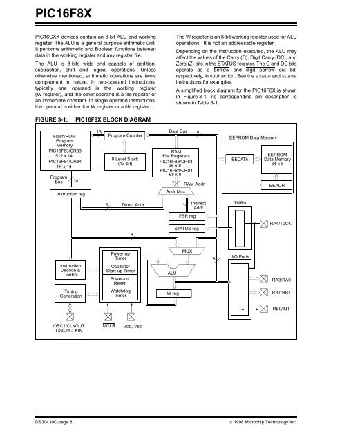
FIGURE 3-1: <strong>PIC16F8X</strong> BLOCK DIAGRAM<br />
Flash/ROM<br />
Program<br />
Memory<br />
PIC16F83/CR83<br />
512 x 14<br />
PIC16F84/CR84<br />
1K x 14<br />
Program<br />
Bus<br />
14<br />
Instruction reg<br />
Instruction<br />
Decode &<br />
Control<br />
Timing<br />
Generation<br />
OSC2/CLKOUT<br />
OSC1/CLKIN<br />
13<br />
5<br />
Program Counter<br />
8 Level Stack<br />
(13-bit)<br />
Direct Addr<br />
8<br />
Power-up<br />
Timer<br />
Oscillator<br />
Start-up Timer<br />
Power-on<br />
Reset<br />
Watchdog<br />
Timer<br />
MCLR VDD, VSS<br />
The W register is an 8-bit working register used for ALU<br />
operations. It is not an addressable register.<br />
Depending on the instruction executed, the ALU may<br />
affect the values of the Carry (C), Digit Carry (DC), and<br />
Zero (Z) bits in the STATUS register. The C and DC bits<br />
operate as a borrow and digit borrow out bit,<br />
respectively, in subtraction. See the SUBLW and SUBWF<br />
instructions for examples.<br />
A simplified block diagram for the <strong>PIC16F8X</strong> is shown<br />
in Figure 3-1, its corresponding pin description is<br />
shown in Table 3-1.<br />
<strong>Data</strong> Bus<br />
RAM<br />
File Registers<br />
PIC16F83/CR83<br />
36 x 8<br />
PIC16F84/CR84<br />
68 x 8<br />
DS30430C-page 8 © 1998 <strong>Microchip</strong> Technology Inc.<br />
7<br />
Addr Mux<br />
ALU<br />
W reg<br />
7<br />
RAM Addr<br />
FSR reg<br />
STATUS reg<br />
MUX<br />
8<br />
Indirect<br />
Addr<br />
8<br />
<strong>EEPROM</strong> <strong>Data</strong> Memory<br />
EEDATA<br />
TMR0<br />
I/O Ports<br />
<strong>EEPROM</strong><br />
<strong>Data</strong> Memory<br />
64 x 8<br />
EEADR<br />
RA4/T0CKI<br />
RA3:RA0<br />
RB7:RB1<br />
RB0/INT


