

PIC16F8X, 18-Pin FLASH/EEPROM 8-Bit MCU Data Sheet - Microchip
PIC16F8X, 18-Pin FLASH/EEPROM 8-Bit MCU Data Sheet - Microchip
PIC16F8X, 18-Pin FLASH/EEPROM 8-Bit MCU Data Sheet - Microchip

You also want an ePaper? Increase the reach of your titles
YUMPU automatically turns print PDFs into web optimized ePapers that Google loves.
5.3 I/O Programming Considerations<br />
5.3.1 BI-DIRECTIONAL I/O PORTS<br />
Any instruction which writes, operates internally as a<br />
read followed by a write operation. The BCF and BSF<br />
instructions, for example, read the register into the<br />
CPU, execute the bit operation and write the result back<br />
to the register. Caution must be used when these<br />
instructions are applied to a port with both inputs and<br />
outputs defined. For example, a BSF operation on bit5<br />
of PORTB will cause all eight bits of PORTB to be read<br />
into the CPU. Then the BSF operation takes place on<br />
bit5 and PORTB is written to the output latches. If<br />
another bit of PORTB is used as a bi-directional I/O pin<br />
(i.e., bit0) and it is defined as an input at this time, the<br />
input signal present on the pin itself would be read into<br />
the CPU and rewritten to the data latch of this particular<br />
pin, overwriting the previous content. As long as the pin<br />
stays in the input mode, no problem occurs. However, if<br />
bit0 is switched into output mode later on, the content<br />
of the data latch is unknown.<br />
Reading the port register, reads the values of the port<br />
pins. Writing to the port register writes the value to the<br />
port latch. When using read-modify-write instructions<br />
(i.e., BCF, BSF, etc.) on a port, the value of the port<br />
pins is read, the desired operation is done to this value,<br />
and this value is then written to the port latch.<br />
A pin actively outputting a Low or High should not be<br />
driven from external devices at the same time in order<br />
to change the level on this pin (“wired-or”, “wired-and”).<br />
The resulting high output current may damage the chip.<br />
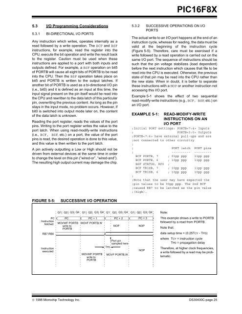
FIGURE 5-5: SUCCESSIVE I/O OPERATION<br />
PC<br />
Instruction<br />
fetched<br />
RB7:RB0<br />
Instruction<br />
executed<br />
Q1 Q2 Q3 Q4 Q1 Q2 Q3 Q4 Q1 Q2 Q3 Q4 Q1 Q2 Q3 Q4<br />
PC PC + 1 PC + 2 PC + 3<br />
MOVWF PORTB<br />
write to<br />
PORTB<br />
MOVF PORTB,W<br />
MOVWF PORTB<br />
write to<br />
PORTB<br />
TPD<br />
NOP<br />
Port pin<br />
sampled here<br />
MOVF PORTB,W<br />
<strong>PIC16F8X</strong><br />
5.3.2 SUCCESSIVE OPERATIONS ON I/O<br />
PORTS<br />
The actual write to an I/O port happens at the end of an<br />
instruction cycle, whereas for reading, the data must be<br />
valid at the beginning of the instruction cycle<br />
(Figure 5-5). Therefore, care must be exercised if a<br />
write followed by a read operation is carried out on the<br />
same I/O port. The sequence of instructions should be<br />
such that the pin voltage stabilizes (load dependent)<br />
before the next instruction which causes that file to be<br />
read into the CPU is executed. Otherwise, the previous<br />
state of that pin may be read into the CPU rather than<br />
the new state. When in doubt, it is better to separate<br />
these instructions with a NOP or another instruction not<br />
accessing this I/O port.<br />
Example 5-1 shows the effect of two sequential<br />
read-modify-write instructions (e.g., BCF, BSF, etc.) on<br />
an I/O port.<br />
EXAMPLE 5-1: READ-MODIFY-WRITE<br />
INSTRUCTIONS ON AN<br />
I/O PORT<br />
;Initial PORT settings: PORTB Inputs<br />
; PORTB Outputs<br />
;PORTB have external pull-ups and are<br />
;not connected to other circuitry<br />
;<br />
; PORT latch PORT pins<br />
; ---------- ---------<br />
BCF PORTB, 7 ; 01pp ppp 11pp ppp<br />
BCF PORTB, 6 ; 10pp ppp 11pp ppp<br />
BSF STATUS, RP0 ;<br />
BCF TRISB, 7 ; 10pp ppp 11pp ppp<br />
BCF TRISB, 6 ; 10pp ppp 10pp ppp<br />
;<br />
;Note that the user may have expected the<br />
;pin values to be 00pp ppp. The 2nd BCF<br />
;caused RB7 to be latched as the pin value<br />
;(high).<br />
© 1998 <strong>Microchip</strong> Technology Inc. DS30430C-page 25<br />
NOP<br />
NOP<br />
Note:<br />
This example shows a write to PORTB<br />
followed by a read from PORTB.<br />
Note that:<br />
data setup time = (0.25TCY - TPD)<br />
where TCY = instruction cycle<br />
TPD = propagation delay<br />
Therefore, at higher clock frequencies,<br />
a write followed by a read may be problematic.


