

PIC16F8X, 18-Pin FLASH/EEPROM 8-Bit MCU Data Sheet - Microchip
PIC16F8X, 18-Pin FLASH/EEPROM 8-Bit MCU Data Sheet - Microchip
PIC16F8X, 18-Pin FLASH/EEPROM 8-Bit MCU Data Sheet - Microchip

Create successful ePaper yourself
Turn your PDF publications into a flip-book with our unique Google optimized e-Paper software.
7.5 Write Verify<br />
Depending on the application, good programming practice<br />
may dictate that the value written to the <strong>Data</strong><br />
<strong>EEPROM</strong> should be verified (Example 7-1) to the<br />
desired value to be written. This should be used in<br />
applications where an <strong>EEPROM</strong> bit will be stressed<br />
near the specification limit. The Total Endurance disk<br />
will help determine your comfort level.<br />
Generally the <strong>EEPROM</strong> write failure will be a bit which<br />
was written as a ’1’, but reads back as a ’0’ (due to<br />
leakage off the bit).<br />
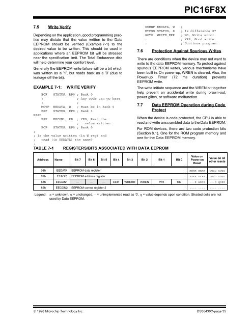
EXAMPLE 7-1: WRITE VERIFY<br />
BCF STATUS, RP0 ; Bank 0<br />
: ; Any code can go here<br />
: ;<br />
MOVF EEDATA, W ; Must be in Bank 0<br />
BSF STATUS, RP0 ; Bank 1<br />
READ<br />
BSF EECON1, RD ; YES, Read the<br />
; value written<br />
BCF STATUS, RP0 ; Bank 0<br />
;<br />
; Is the value written (in W reg) and<br />
; read (in EEDATA) the same?<br />
;<br />
TABLE 7-1 REGISTERS/BITS ASSOCIATED WITH DATA <strong>EEPROM</strong><br />
<strong>PIC16F8X</strong><br />
SUBWF EEDATA, W ;<br />
BTFSS STATUS, Z ; Is difference 0?<br />
GOTO WRITE_ERR ; NO, Write error<br />
: ; YES, Good write<br />
: ; Continue program<br />
7.6 Protection Against Spurious Writes<br />
There are conditions when the device may not want to<br />
write to the data <strong>EEPROM</strong> memory. To protect against<br />
spurious <strong>EEPROM</strong> writes, various mechanisms have<br />
been built in. On power-up, WREN is cleared. Also, the<br />
Power-up Timer (72 ms duration) prevents<br />
<strong>EEPROM</strong> write.<br />
The write initiate sequence and the WREN bit together<br />
help prevent an accidental write during brown-out,<br />
power glitch, or software malfunction.<br />
7.7 <strong>Data</strong> <strong>EEPROM</strong> Operation during Code<br />
Protect<br />
When the device is code protected, the CPU is able to<br />
read and write unscrambled data to the <strong>Data</strong> <strong>EEPROM</strong>.<br />
For ROM devices, there are two code protection bits<br />
(Section 8.1). One for the ROM program memory and<br />
one for the <strong>Data</strong> <strong>EEPROM</strong> memory.<br />
Address Name <strong>Bit</strong> 7 <strong>Bit</strong> 6 <strong>Bit</strong> 5 <strong>Bit</strong> 4 <strong>Bit</strong> 3 <strong>Bit</strong> 2 <strong>Bit</strong> 1 <strong>Bit</strong> 0<br />
Value on<br />
Power-on<br />
Reset<br />
Value on all<br />
other resets<br />
08h EEDATA <strong>EEPROM</strong> data register xxxx xxxx uuuu uuuu<br />
09h EEADR <strong>EEPROM</strong> address register xxxx xxxx uuuu uuuu<br />
88h EECON1 — — — EEIF WRERR WREN WR RD ---0 x000 ---0 q000<br />
89h EECON2 <strong>EEPROM</strong> control register 2 ---- ---- ---- ----<br />
Legend: x = unknown, u = unchanged, - = unimplemented read as ’0’, q = value depends upon condition. Shaded cells are not<br />
used by <strong>Data</strong> <strong>EEPROM</strong>.<br />
© 1998 <strong>Microchip</strong> Technology Inc. DS30430C-page 35


