

PIC16F8X, 18-Pin FLASH/EEPROM 8-Bit MCU Data Sheet - Microchip
PIC16F8X, 18-Pin FLASH/EEPROM 8-Bit MCU Data Sheet - Microchip
PIC16F8X, 18-Pin FLASH/EEPROM 8-Bit MCU Data Sheet - Microchip

You also want an ePaper? Increase the reach of your titles
YUMPU automatically turns print PDFs into web optimized ePapers that Google loves.
<strong>PIC16F8X</strong> PIC16CR83/84<br />
12.5 Timing Diagrams and Specifications<br />
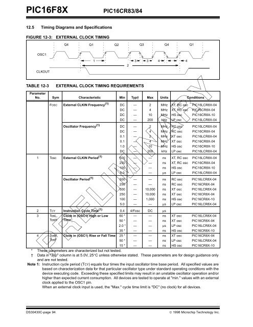
FIGURE 12-3: EXTERNAL CLOCK TIMING<br />
OSC1<br />
CLKOUT<br />
Q4 Q1 Q2 Q3 Q4 Q1<br />
1 3 3 4 4<br />
2<br />
TABLE 12-3 EXTERNAL CLOCK TIMING REQUIREMENTS<br />
Parameter<br />
No. Sym Characteristic Min Typ† Max Units Conditions<br />
FOSC External CLKIN Frequency (1)<br />
DC — 2 MHz XT, RC osc PIC16LCR8X-04<br />
DC — 4 MHz XT, RC osc PIC16CR8X-04<br />
DC — 10 MHz HS osc PIC16CR8X-10<br />
DC — 200 kHz LP osc PIC16LCR8X-04<br />
Oscillator Frequency (1)<br />
DC — 2 MHz RC osc PIC16LCR8X-04<br />
DC — 4 MHz RC osc PIC16CR8X-04<br />
0.1 — 2 MHz XT osc PIC16LCR8X-04<br />
0.1 — 4 MHz XT osc PIC16CR8X-04<br />
1.0 — 10 MHz HS osc PIC16CR8X-10<br />
DC — 200 kHz LP osc PIC16LCR8X-04<br />
1 Tosc External CLKIN Period (1)<br />
500 — — ns XT, RC osc PIC16LCR8X-04<br />
250 — — ns XT, RC osc PIC16CR8X-04<br />
100 — — ns HS osc PIC16CR8X-10<br />
5.0 — — μs LP osc PIC16LCR8X-04<br />
Oscillator Period (1)<br />
500 — — ns RC osc PIC16LCR8X-04<br />
250 — — ns RC osc PIC16CR8X-04<br />
500 — 10,000 ns XT osc PIC16LCR8X-04<br />
250 — 10,000 ns XT osc PIC16CR8X-04<br />
100 — 1,000 ns HS osc PIC16CR8X-10<br />
5.0 — — μs LP osc PIC16LCR8X-04<br />
2 TCY Instruction Cycle Time (1)<br />
0.4 4/Fosc DC μs<br />
3 TosL, Clock in (OSC1) High or Low 60 * — — ns XT osc PIC16LCR8X-04<br />
TosH Time<br />
50 * — — ns XT osc PIC16CR8X-04<br />
2.0 * — — μs LP osc PIC16LCR8X-04<br />
35 * — — ns HS osc PIC16CR8X-10<br />
4 TosR, Clock in (OSC1) Rise or Fall Time 25 * — — ns XT osc PIC16CR8X-04<br />
TosF<br />
50 * — — ns LP osc PIC16LCR8X-04<br />
15 * — — ns HS osc PIC16CR8X-10<br />
* These parameters are characterized but not tested.<br />
† <strong>Data</strong> in "Typ" column is at 5.0V, 25°C unless otherwise stated. These parameters are for design guidance only<br />
and are not tested.<br />
Note 1: Instruction cycle period (TCY) equals four times the input oscillator time base period. All specified values are<br />
based on characterization data for that particular oscillator type under standard operating conditions with the<br />
device executing code. Exceeding these specified limits may result in an unstable oscillator operation and/or<br />
higher than expected current consumption. All devices are tested to operate at "min." values with an external<br />
clock applied to the OSC1 pin.<br />
When an external clock input is used, the "Max." cycle time limit is "DC" (no clock) for all devices.<br />
DS30430C-page 94 © 1998 <strong>Microchip</strong> Technology Inc.


