

PIC16F8X, 18-Pin FLASH/EEPROM 8-Bit MCU Data Sheet - Microchip
PIC16F8X, 18-Pin FLASH/EEPROM 8-Bit MCU Data Sheet - Microchip
PIC16F8X, 18-Pin FLASH/EEPROM 8-Bit MCU Data Sheet - Microchip

Create successful ePaper yourself
Turn your PDF publications into a flip-book with our unique Google optimized e-Paper software.
6.0 TIMER0 MODULE AND TMR0<br />
REGISTER<br />
The Timer0 module timer/counter has the following<br />
features:<br />
• 8-bit timer/counter<br />
• Readable and writable<br />
• 8-bit software programmable prescaler<br />
• Internal or external clock select<br />
• Interrupt on overflow from FFh to 00h<br />
• Edge select for external clock<br />
Timer mode is selected by clearing the T0CS bit<br />
(OPTION_REG). In timer mode, the Timer0 module<br />
(Figure 6-1) will increment every instruction cycle<br />
(without prescaler). If the TMR0 register is written, the<br />
increment is inhibited for the following two cycles<br />
(Figure 6-2 and Figure 6-3). The user can work around<br />
this by writing an adjusted value to the TMR0 register.<br />
Counter mode is selected by setting the T0CS bit<br />
(OPTION_REG). In this mode TMR0 will increment<br />
either on every rising or falling edge of pin RA4/T0CKI.<br />
The incrementing edge is determined by the T0 source<br />
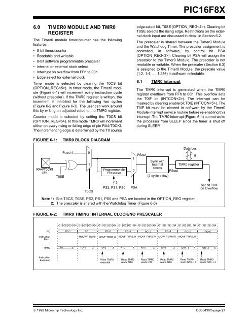
FIGURE 6-1: TMR0 BLOCK DIAGRAM<br />
RA4/T0CKI<br />
pin<br />
T0SE<br />
FOSC/4<br />
0<br />
1<br />
T0CS<br />
Programmable<br />
Prescaler<br />
<strong>PIC16F8X</strong><br />
edge select bit, T0SE (OPTION_REG). Clearing bit<br />
T0SE selects the rising edge. Restrictions on the external<br />
clock input are discussed in detail in Section 6.2.<br />
The prescaler is shared between the Timer0 Module<br />
and the Watchdog Timer. The prescaler assignment is<br />
controlled, in software, by control bit PSA<br />
(OPTION_REG). Clearing bit PSA will assign the<br />
prescaler to the Timer0 Module. The prescaler is not<br />
readable or writable. When the prescaler (Section 6.3)<br />
is assigned to the Timer0 Module, the prescale value<br />
(1:2, 1:4, ..., 1:256) is software selectable.<br />
6.1 TMR0 Interrupt<br />
FIGURE 6-2: TMR0 TIMING: INTERNAL CLOCK/NO PRESCALER<br />
The TMR0 interrupt is generated when the TMR0<br />
register overflows from FFh to 00h. This overflow sets<br />
the T0IF bit (INTCON). The interrupt can be<br />
masked by clearing enable bit T0IE (INTCON). The<br />
T0IF bit must be cleared in software by the Timer0<br />
Module interrupt service routine before re-enabling this<br />
interrupt. The TMR0 interrupt (Figure 6-4) cannot wake<br />
the processor from SLEEP since the timer is shut off<br />
during SLEEP.<br />
Note 1: <strong>Bit</strong>s T0CS, T0SE, PS2, PS1, PS0 and PSA are located in the OPTION_REG register.<br />
2: The prescaler is shared with the Watchdog Timer (Figure 6-6)<br />
PC<br />
Instruction<br />
Fetch<br />
TMR0<br />
Instruction<br />
Executed<br />
PC-1<br />
3<br />
PS2, PS1, PS0<br />
© 1998 <strong>Microchip</strong> Technology Inc. DS30430C-page 27<br />
1<br />
0<br />
PSA<br />
<strong>Data</strong> bus<br />
PSout<br />
8<br />
Sync with<br />
Internal TMR0 register<br />
clocks<br />
PSout<br />
(2 cycle delay)<br />
Set bit T0IF<br />
on Overflow<br />
Q1 Q2 Q3 Q4 Q1 Q2 Q3 Q4 Q1 Q2 Q3 Q4 Q1 Q2 Q3 Q4 Q1 Q2 Q3 Q4 Q1 Q2 Q3 Q4 Q1 Q2 Q3 Q4 Q1 Q2 Q3 Q4<br />
PC PC+1 PC+2 PC+3 PC+4 PC+5 PC+6<br />
MOVWF TMR0 MOVF TMR0,W MOVF TMR0,W MOVF TMR0,W MOVF TMR0,W MOVF TMR0,W<br />
T0 T0+1 T0+2 NT0 NT0 NT0 NT0+1 NT0+2 T0<br />
Write TMR0<br />
executed<br />
Read TMR0<br />
reads NT0<br />
Read TMR0<br />
reads NT0<br />
Read TMR0<br />
reads NT0<br />
Read TMR0<br />
reads NT0 + 1<br />
Read TMR0<br />
reads NT0 + 2


