

PIC16F8X, 18-Pin FLASH/EEPROM 8-Bit MCU Data Sheet - Microchip
PIC16F8X, 18-Pin FLASH/EEPROM 8-Bit MCU Data Sheet - Microchip
PIC16F8X, 18-Pin FLASH/EEPROM 8-Bit MCU Data Sheet - Microchip

You also want an ePaper? Increase the reach of your titles
YUMPU automatically turns print PDFs into web optimized ePapers that Google loves.
4.0 MEMORY ORGANIZATION<br />
There are two memory blocks in the <strong>PIC16F8X</strong>. These<br />
are the program memory and the data memory. Each<br />
block has its own bus, so that access to each block can<br />
occur during the same oscillator cycle.<br />
The data memory can further be broken down into the<br />
general purpose RAM and the Special Function<br />
Registers (SFRs). The operation of the SFRs that<br />
control the “core” are described here. The SFRs used<br />
to control the peripheral modules are described in the<br />
section discussing each individual peripheral module.<br />
The data memory area also contains the data<br />
<strong>EEPROM</strong> memory. This memory is not directly mapped<br />
into the data memory, but is indirectly mapped. That is,<br />
an indirect address pointer specifies the address of the<br />
data <strong>EEPROM</strong> memory to read/write. The 64 bytes of<br />
data <strong>EEPROM</strong> memory have the address range<br />
0h-3Fh. More details on the <strong>EEPROM</strong> memory can be<br />
found in Section 7.0.<br />
4.1 Program Memory Organization<br />
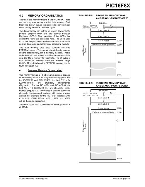
The PIC16FXX has a 13-bit program counter capable<br />
of addressing an 8K x 14 program memory space. For<br />
the PIC16F83 and PIC16CR83, the first 512 x 14<br />
(0000h-01FFh) are physically implemented<br />
(Figure 4-1). For the PIC16F84 and PIC16CR84, the<br />
first 1K x 14 (0000h-03FFh) are physically implemented<br />
(Figure 4-2). Accessing a location above the<br />
physically implemented address will cause a wraparound.<br />
For example, for the PIC16F84 locations 20h,<br />
420h, 820h, C20h, 1020h, 1420h, <strong>18</strong>20h, and 1C20h<br />
will be the same instruction.<br />
The reset vector is at 0000h and the interrupt vector is<br />
at 0004h.<br />
<strong>PIC16F8X</strong><br />
FIGURE 4-1: PROGRAM MEMORY MAP<br />
AND STACK - PIC16F83/CR83<br />
PC<br />
CALL, RETURN<br />
13<br />
RETFIE, RETLW<br />
Stack Level 1<br />
FIGURE 4-2: PROGRAM MEMORY MAP<br />
AND STACK - PIC16F84/CR84<br />
© 1998 <strong>Microchip</strong> Technology Inc. DS30430C-page 11<br />
User Memory<br />
Space<br />
•<br />
Stack Level 8<br />
Reset Vector<br />
Peripheral Interrupt Vector<br />
PC<br />
CALL, RETURN<br />
13<br />
RETFIE, RETLW<br />
Stack Level 1<br />
User Memory<br />
Space<br />
•<br />
Stack Level 8<br />
Reset Vector<br />
Peripheral Interrupt Vector<br />
0000h<br />
0004h<br />
1FFh<br />
1FFFh<br />
0000h<br />
0004h<br />
3FFh<br />
1FFFh


