

PIC16F8X, 18-Pin FLASH/EEPROM 8-Bit MCU Data Sheet - Microchip
PIC16F8X, 18-Pin FLASH/EEPROM 8-Bit MCU Data Sheet - Microchip
PIC16F8X, 18-Pin FLASH/EEPROM 8-Bit MCU Data Sheet - Microchip

You also want an ePaper? Increase the reach of your titles
YUMPU automatically turns print PDFs into web optimized ePapers that Google loves.
4.5 Indirect Addressing; INDF and FSR<br />
Registers<br />
The INDF register is not a physical register. Addressing<br />
INDF actually addresses the register whose<br />
address is contained in the FSR register (FSR is a<br />
pointer). This is indirect addressing.<br />
EXAMPLE 4-1: INDIRECT ADDRESSING<br />
• Register file 05 contains the value 10h<br />
• Register file 06 contains the value 0Ah<br />
• Load the value 05 into the FSR register<br />
• A read of the INDF register will return the value of<br />
10h<br />
• Increment the value of the FSR register by one<br />
(FSR = 06)<br />
• A read of the INDF register now will return the<br />
value of 0Ah.<br />
Reading INDF itself indirectly (FSR = 0) will produce<br />
00h. Writing to the INDF register indirectly results in a<br />
no-operation (although STATUS bits may be affected).<br />
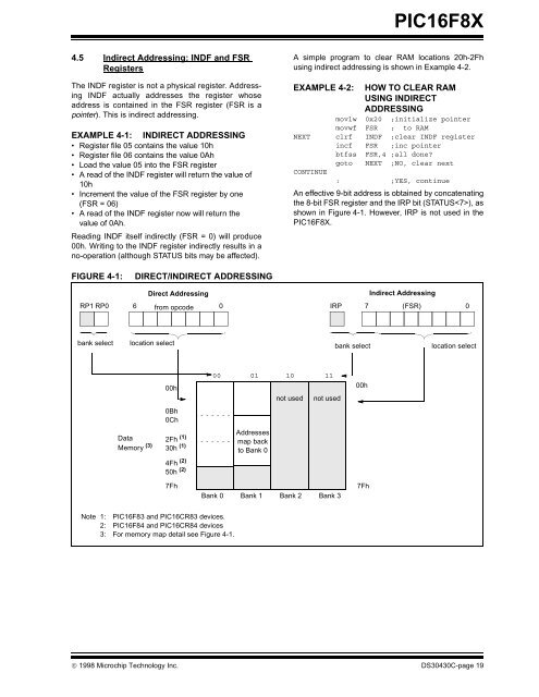
FIGURE 4-1: DIRECT/INDIRECT ADDRESSING<br />
<strong>PIC16F8X</strong><br />
A simple program to clear RAM locations 20h-2Fh<br />
using indirect addressing is shown in Example 4-2.<br />
EXAMPLE 4-2: HOW TO CLEAR RAM<br />
USING INDIRECT<br />
ADDRESSING<br />
movlw 0x20 ;initialize pointer<br />
movwf FSR ; to RAM<br />
NEXT clrf INDF ;clear INDF register<br />
incf FSR ;inc pointer<br />
btfss FSR,4 ;all done?<br />
goto NEXT ;NO, clear next<br />
CONTINUE<br />
: ;YES, continue<br />
An effective 9-bit address is obtained by concatenating<br />
the 8-bit FSR register and the IRP bit (STATUS), as<br />
shown in Figure 4-1. However, IRP is not used in the<br />
<strong>PIC16F8X</strong>.<br />
Direct Addressing<br />
Indirect Addressing<br />
RP1 RP0 6 from opcode 0 IRP 7 (FSR) 0<br />
bank select location select<br />
<strong>Data</strong><br />
Memory (3)<br />
00h<br />
0Bh<br />
0Ch<br />
2Fh (1)<br />
30h (1)<br />
4Fh<br />
7Fh<br />
(2)<br />
50h (2)<br />
Note 1: PIC16F83 and PIC16CR83 devices.<br />
2: PIC16F84 and PIC16CR84 devices<br />
3: For memory map detail see Figure 4-1.<br />
00 01 10 11<br />
Addresses<br />
map back<br />
to Bank 0<br />
not used<br />
not used<br />
Bank 0 Bank 1 Bank 2 Bank 3<br />
bank select location select<br />
© 1998 <strong>Microchip</strong> Technology Inc. DS30430C-page 19<br />
00h<br />
7Fh


