

PIC16F8X, 18-Pin FLASH/EEPROM 8-Bit MCU Data Sheet - Microchip
PIC16F8X, 18-Pin FLASH/EEPROM 8-Bit MCU Data Sheet - Microchip
PIC16F8X, 18-Pin FLASH/EEPROM 8-Bit MCU Data Sheet - Microchip

You also want an ePaper? Increase the reach of your titles
YUMPU automatically turns print PDFs into web optimized ePapers that Google loves.
<strong>PIC16F8X</strong><br />
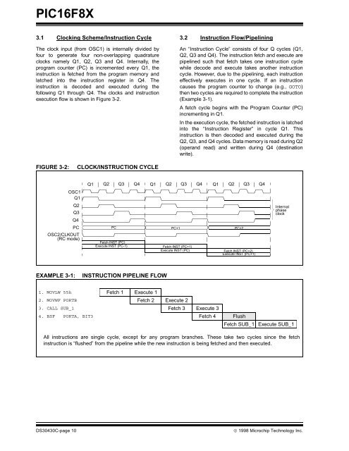
3.1 Clocking Scheme/Instruction Cycle<br />
The clock input (from OSC1) is internally divided by<br />
four to generate four non-overlapping quadrature<br />
clocks namely Q1, Q2, Q3 and Q4. Internally, the<br />
program counter (PC) is incremented every Q1, the<br />
instruction is fetched from the program memory and<br />
latched into the instruction register in Q4. The<br />
instruction is decoded and executed during the<br />
following Q1 through Q4. The clocks and instruction<br />
execution flow is shown in Figure 3-2.<br />
FIGURE 3-2: CLOCK/INSTRUCTION CYCLE<br />
OSC1<br />
Q1<br />
Q2<br />
Q3<br />
Q4<br />
PC<br />
OSC2/CLKOUT<br />
(RC mode)<br />
EXAMPLE 3-1: INSTRUCTION PIPELINE FLOW<br />
3.2 Instruction Flow/Pipelining<br />
An “Instruction Cycle” consists of four Q cycles (Q1,<br />
Q2, Q3 and Q4). The instruction fetch and execute are<br />
pipelined such that fetch takes one instruction cycle<br />
while decode and execute takes another instruction<br />
cycle. However, due to the pipelining, each instruction<br />
effectively executes in one cycle. If an instruction<br />
causes the program counter to change (e.g., GOTO)<br />
then two cycles are required to complete the instruction<br />
(Example 3-1).<br />
A fetch cycle begins with the Program Counter (PC)<br />
incrementing in Q1.<br />
In the execution cycle, the fetched instruction is latched<br />
into the “Instruction Register” in cycle Q1. This<br />
instruction is then decoded and executed during the<br />
Q2, Q3, and Q4 cycles. <strong>Data</strong> memory is read during Q2<br />
(operand read) and written during Q4 (destination<br />
write).<br />
Q1 Q2 Q3 Q4 Q1 Q2 Q3 Q4 Q1 Q2 Q3 Q4<br />
PC PC+1 PC+2<br />
Fetch INST (PC)<br />
Execute INST (PC-1) Fetch INST (PC+1)<br />
Execute INST (PC) Fetch INST (PC+2)<br />
Execute INST (PC+1)<br />
Internal<br />
phase<br />
clock<br />
1. MOVLW 55h Fetch 1 Execute 1<br />
2. MOVWF PORTB Fetch 2 Execute 2<br />
3. CALL SUB_1 Fetch 3 Execute 3<br />
4. BSF PORTA, BIT3 Fetch 4 Flush<br />
Fetch SUB_1 Execute SUB_1<br />
All instructions are single cycle, except for any program branches. These take two cycles since the fetch<br />
instruction is “flushed” from the pipeline while the new instruction is being fetched and then executed.<br />
DS30430C-page 10 © 1998 <strong>Microchip</strong> Technology Inc.


