

PIC16F8X, 18-Pin FLASH/EEPROM 8-Bit MCU Data Sheet - Microchip
PIC16F8X, 18-Pin FLASH/EEPROM 8-Bit MCU Data Sheet - Microchip
PIC16F8X, 18-Pin FLASH/EEPROM 8-Bit MCU Data Sheet - Microchip

You also want an ePaper? Increase the reach of your titles
YUMPU automatically turns print PDFs into web optimized ePapers that Google loves.
4.2.2.1 STATUS REGISTER<br />
The STATUS register contains the arithmetic status of<br />
the ALU, the RESET status and the bank select bit for<br />
data memory.<br />
As with any register, the STATUS register can be the<br />
destination for any instruction. If the STATUS register is<br />
the destination for an instruction that affects the Z, DC<br />
or C bits, then the write to these three bits is disabled.<br />
These bits are set or cleared according to device logic.<br />
Furthermore, the TO and PD bits are not writable.<br />
Therefore, the result of an instruction with the STATUS<br />
register as destination may be different than intended.<br />
For example, CLRF STATUS will clear the upper-three<br />
bits and set the Z bit. This leaves the STATUS register<br />
as 000u u1uu (where u = unchanged).<br />
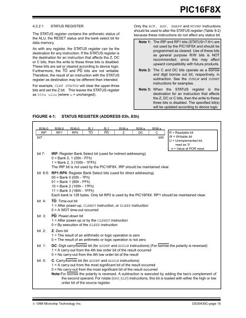
FIGURE 4-1: STATUS REGISTER (ADDRESS 03h, 83h)<br />
<strong>PIC16F8X</strong><br />
Only the BCF, BSF, SWAPF and MOVWF instructions<br />
should be used to alter the STATUS register (Table 9-2)<br />
because these instructions do not affect any status bit.<br />
Note 1: The IRP and RP1 bits (STATUS) are<br />
not used by the <strong>PIC16F8X</strong> and should be<br />
programmed as cleared. Use of these bits<br />
as general purpose R/W bits is NOT<br />
recommended, since this may affect<br />
upward compatibility with future products.<br />
Note 2: The C and DC bits operate as a borrow<br />
and digit borrow out bit, respectively, in<br />
subtraction. See the SUBLW and SUBWF<br />
instructions for examples.<br />
Note 3: When the STATUS register is the<br />
destination for an instruction that affects<br />
the Z, DC or C bits, then the write to these<br />
three bits is disabled. The specified bit(s)<br />
will be updated according to device logic<br />
R/W-0 R/W-0 R/W-0 R-1 R-1 R/W-x R/W-x R/W-x<br />
IRP RP1 RP0 TO PD Z DC C R = Readable bit<br />
bit7 bit0 W = Writable bit<br />
U = Unimplemented bit,<br />
read as ‘0’<br />
- n = Value at POR reset<br />
bit 7: IRP: Register Bank Select bit (used for indirect addressing)<br />
0 = Bank 0, 1 (00h - FFh)<br />
1 = Bank 2, 3 (100h - 1FFh)<br />
The IRP bit is not used by the <strong>PIC16F8X</strong>. IRP should be maintained clear.<br />
bit 6-5: RP1:RP0: Register Bank Select bits (used for direct addressing)<br />
00 = Bank 0 (00h - 7Fh)<br />
01 = Bank 1 (80h - FFh)<br />
10 = Bank 2 (100h - 17Fh)<br />
11 = Bank 3 (<strong>18</strong>0h - 1FFh)<br />
Each bank is 128 bytes. Only bit RP0 is used by the <strong>PIC16F8X</strong>. RP1 should be maintained clear.<br />
bit 4: TO: Time-out bit<br />
1 = After power-up, CLRWDT instruction, or SLEEP instruction<br />
0 = A WDT time-out occurred<br />
bit 3: PD: Power-down bit<br />
1 = After power-up or by the CLRWDT instruction<br />
0 = By execution of the SLEEP instruction<br />
bit 2: Z: Zero bit<br />
1 = The result of an arithmetic or logic operation is zero<br />
0 = The result of an arithmetic or logic operation is not zero<br />
bit 1: DC: Digit carry/borrow bit (for ADDWF and ADDLW instructions) (For borrow the polarity is reversed)<br />
1 = A carry-out from the 4th low order bit of the result occurred<br />
0 = No carry-out from the 4th low order bit of the result<br />
bit 0: C: Carry/borrow bit (for ADDWF and ADDLW instructions)<br />
1 = A carry-out from the most significant bit of the result occurred<br />
0 = No carry-out from the most significant bit of the result occurred<br />
Note:For borrow the polarity is reversed. A subtraction is executed by adding the two’s complement of<br />
the second operand. For rotate (RRF, RLF) instructions, this bit is loaded with either the high or low<br />
order bit of the source register.<br />
© 1998 <strong>Microchip</strong> Technology Inc. DS30430C-page 15


