PIC16F8X, 18-Pin FLASH/EEPROM 8-Bit MCU Data Sheet - Microchip
PIC16F8X, 18-Pin FLASH/EEPROM 8-Bit MCU Data Sheet - Microchip
PIC16F8X, 18-Pin FLASH/EEPROM 8-Bit MCU Data Sheet - Microchip
You also want an ePaper? Increase the reach of your titles
YUMPU automatically turns print PDFs into web optimized ePapers that Google loves.
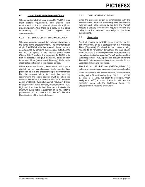
6.2 Using TMR0 with External Clock<br />
When an external clock input is used for TMR0, it must<br />
meet certain requirements. The external clock<br />
requirement is due to internal phase clock (TOSC)<br />
synchronization. Also, there is a delay in the actual<br />
incrementing of the TMR0 register after<br />
synchronization.<br />
6.2.1 EXTERNAL CLOCK SYNCHRONIZATION<br />
When no prescaler is used, the external clock input is<br />
the same as the prescaler output. The synchronization<br />
of pin RA4/T0CKI with the internal phase clocks is<br />
accomplished by sampling the prescaler output on the<br />
Q2 and Q4 cycles of the internal phase clocks<br />
(Figure 6-5). Therefore, it is necessary for T0CKI to be<br />
high for at least 2Tosc (plus a small RC delay) and low<br />
for at least 2Tosc (plus a small RC delay). Refer to the<br />
electrical specification of the desired device.<br />
When a prescaler is used, the external clock input is<br />
divided by an asynchronous ripple counter type<br />
prescaler so that the prescaler output is symmetrical.<br />
For the external clock to meet the sampling<br />
requirement, the ripple counter must be taken into<br />
account. Therefore, it is necessary for T0CKI to have a<br />
period of at least 4Tosc (plus a small RC delay) divided<br />
by the prescaler value. The only requirement on T0CKI<br />
high and low time is that they do not violate the<br />
minimum pulse width requirement of 10 ns. Refer to<br />
parameters 40, 41 and 42 in the AC Electrical<br />
Specifications of the desired device.<br />
6.2.2 TMR0 INCREMENT DELAY<br />
<strong>PIC16F8X</strong><br />
Since the prescaler output is synchronized with the<br />
internal clocks, there is a small delay from the time the<br />
external clock edge occurs to the time the Timer0<br />
Module is actually incremented. Figure 6-5 shows the<br />
delay from the external clock edge to the timer<br />
incrementing.<br />
6.3 Prescaler<br />
An 8-bit counter is available as a prescaler for the<br />
Timer0 Module, or as a postscaler for the Watchdog<br />
Timer (Figure 6-6). For simplicity, this counter is being<br />
referred to as “prescaler” throughout this data sheet.<br />
Note that there is only one prescaler available which is<br />
mutually exclusive between the Timer0 Module and the<br />
Watchdog Timer. Thus, a prescaler assignment for the<br />
Timer0 Module means that there is no prescaler for the<br />
Watchdog Timer, and vice-versa.<br />
The PSA and PS2:PS0 bits (OPTION_REG)<br />
determine the prescaler assignment and prescale ratio.<br />
When assigned to the Timer0 Module, all instructions<br />
writing to the Timer0 Module (e.g., CLRF 1, MOVWF<br />
1, BSF 1,x ....etc.) will clear the prescaler. When<br />
assigned to WDT, a CLRWDT instruction will clear the<br />
prescaler along with the Watchdog Timer. The<br />
prescaler is not readable or writable.<br />
© 1998 <strong>Microchip</strong> Technology Inc. DS30430C-page 29


