

PIC16F8X, 18-Pin FLASH/EEPROM 8-Bit MCU Data Sheet - Microchip
PIC16F8X, 18-Pin FLASH/EEPROM 8-Bit MCU Data Sheet - Microchip
PIC16F8X, 18-Pin FLASH/EEPROM 8-Bit MCU Data Sheet - Microchip

Create successful ePaper yourself
Turn your PDF publications into a flip-book with our unique Google optimized e-Paper software.
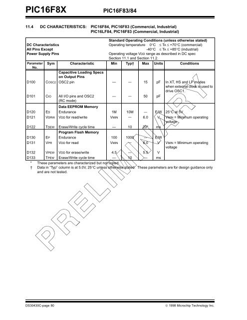
<strong>PIC16F8X</strong> PIC16F83/84<br />
11.4 DC CHARACTERISTICS: PIC16F84, PIC16F83 (Commercial, Industrial)<br />
PIC16LF84, PIC16F83 (Commercial, Industrial)<br />
DC Characteristics<br />
All <strong>Pin</strong>s Except<br />
Power Supply <strong>Pin</strong>s<br />
Standard Operating Conditions (unless otherwise stated)<br />
Operating temperature 0°C ≤ TA ≤ +70°C (commercial)<br />
-40°C ≤ TA ≤ +85°C (industrial)<br />
Operating voltage VDD range as described in DC spec<br />
Section 11.1 and Section 11.2.<br />
Parameter<br />
No.<br />
Sym Characteristic<br />
Capacitive Loading Specs<br />
on Output <strong>Pin</strong>s<br />
Min Typ† Max Units Conditions<br />
D100 COSC2 OSC2 pin — — 15 pF In XT, HS and LP modes<br />
when external clock is used to<br />
drive OSC1.<br />
D101 CIO All I/O pins and OSC2<br />
(RC mode)<br />
<strong>Data</strong> <strong>EEPROM</strong> Memory<br />
— — 50 pF<br />
D120 ED Endurance 1M 10M — E/W 25°C at 5V<br />
D121 VDRW VDD for read/write VMIN — 6.0 V VMIN = Minimum operating<br />
voltage<br />
D122 TDEW Erase/Write cycle time<br />
Program Flash Memory<br />
— 10 20* ms<br />
D130 EP Endurance 100 1000 — E/W<br />
D131 VPR VDD for read VMIN — 6.0 V VMIN = Minimum operating<br />
voltage<br />
D132 VPEW VDD for erase/write 4.5 — 5.5 V<br />
D133 TPEW Erase/Write cycle time — 10 — ms<br />
* These parameters are characterized but not tested.<br />
† <strong>Data</strong> in “Typ” column is at 5.0V, 25°C unless otherwise stated. These parameters are for design guidance only<br />
and are not tested.<br />
DS30430C-page 80 © 1998 <strong>Microchip</strong> Technology Inc.


