

PIC16F8X, 18-Pin FLASH/EEPROM 8-Bit MCU Data Sheet - Microchip
PIC16F8X, 18-Pin FLASH/EEPROM 8-Bit MCU Data Sheet - Microchip
PIC16F8X, 18-Pin FLASH/EEPROM 8-Bit MCU Data Sheet - Microchip

Create successful ePaper yourself
Turn your PDF publications into a flip-book with our unique Google optimized e-Paper software.
<strong>PIC16F8X</strong> PIC16F83/84<br />
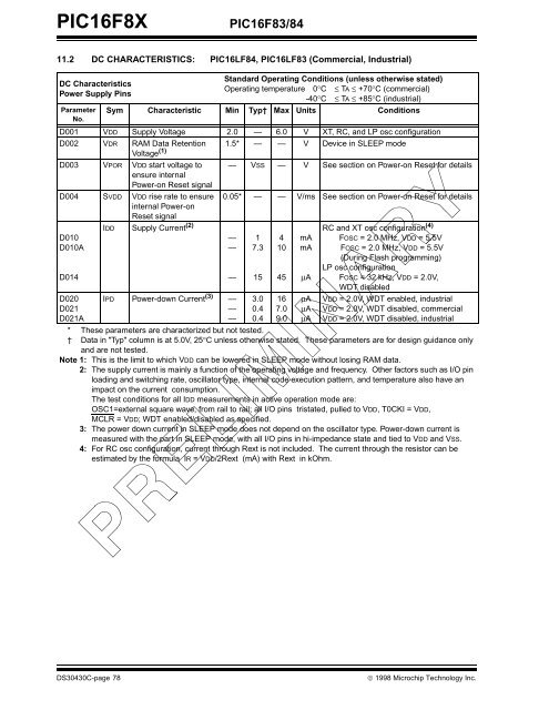
11.2 DC CHARACTERISTICS: PIC16LF84, PIC16LF83 (Commercial, Industrial)<br />
DC Characteristics<br />
Power Supply <strong>Pin</strong>s<br />
D010<br />
D010A<br />
D014<br />
Standard Operating Conditions (unless otherwise stated)<br />
Operating temperature 0°C ≤ TA ≤ +70°C (commercial)<br />
-40°C ≤ TA ≤ +85°C (industrial)<br />
Parameter<br />
No.<br />
Sym Characteristic Min Typ† Max Units Conditions<br />
D001 VDD Supply Voltage 2.0 — 6.0 V XT, RC, and LP osc configuration<br />
D002 VDR RAM <strong>Data</strong> Retention<br />
Voltage (1)<br />
1.5* — — V Device in SLEEP mode<br />
D003 VPOR VDD start voltage to<br />
ensure internal<br />
Power-on Reset signal<br />
— VSS — V See section on Power-on Reset for details<br />
D004 SVDD VDD rise rate to ensure<br />
internal Power-on<br />
Reset signal<br />
0.05* — — V/ms See section on Power-on Reset for details<br />
IDD Supply Current (2)<br />
RC and XT osc configuration (4)<br />
D020<br />
D021<br />
D021A<br />
—<br />
—<br />
—<br />
IPD Power-down Current (3) —<br />
—<br />
—<br />
1<br />
7.3<br />
15<br />
3.0<br />
0.4<br />
0.4<br />
DS30430C-page 78 © 1998 <strong>Microchip</strong> Technology Inc.<br />
4<br />
10<br />
45<br />
16<br />
7.0<br />
9.0<br />
mA<br />
mA<br />
μA<br />
μA<br />
μA<br />
μA<br />
FOSC = 2.0 MHz, VDD = 5.5V<br />
FOSC = 2.0 MHz, VDD = 5.5V<br />
(During Flash programming)<br />
LP osc configuration<br />
FOSC = 32 kHz, VDD = 2.0V,<br />
WDT disabled<br />
VDD = 2.0V, WDT enabled, industrial<br />
VDD = 2.0V, WDT disabled, commercial<br />
VDD = 2.0V, WDT disabled, industrial<br />
* These parameters are characterized but not tested.<br />
† <strong>Data</strong> in "Typ" column is at 5.0V, 25°C unless otherwise stated. These parameters are for design guidance only<br />
and are not tested.<br />
Note 1: This is the limit to which VDD can be lowered in SLEEP mode without losing RAM data.<br />
2: The supply current is mainly a function of the operating voltage and frequency. Other factors such as I/O pin<br />
loading and switching rate, oscillator type, internal code execution pattern, and temperature also have an<br />
impact on the current consumption.<br />
The test conditions for all IDD measurements in active operation mode are:<br />
OSC1=external square wave, from rail to rail; all I/O pins tristated, pulled to VDD, T0CKI = VDD,<br />
MCLR = VDD; WDT enabled/disabled as specified.<br />
3: The power down current in SLEEP mode does not depend on the oscillator type. Power-down current is<br />
measured with the part in SLEEP mode, with all I/O pins in hi-impedance state and tied to VDD and VSS.<br />
4: For RC osc configuration, current through Rext is not included. The current through the resistor can be<br />
estimated by the formula IR = VDD/2Rext (mA) with Rext in kOhm.


