

PIC16F8X, 18-Pin FLASH/EEPROM 8-Bit MCU Data Sheet - Microchip
PIC16F8X, 18-Pin FLASH/EEPROM 8-Bit MCU Data Sheet - Microchip
PIC16F8X, 18-Pin FLASH/EEPROM 8-Bit MCU Data Sheet - Microchip

You also want an ePaper? Increase the reach of your titles
YUMPU automatically turns print PDFs into web optimized ePapers that Google loves.
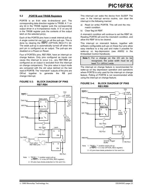
5.2 PORTB and TRISB Registers<br />
PORTB is an 8-bit wide bi-directional port. The<br />
corresponding data direction register is TRISB. A ’1’ on<br />
any bit in the TRISB register puts the corresponding<br />
output driver in a hi-impedance mode. A ’0’ on any bit<br />
in the TRISB register puts the contents of the output<br />
latch on the selected pin(s).<br />
Each of the PORTB pins have a weak internal pull-up.<br />
A single control bit can turn on all the pull-ups. This is<br />
done by clearing the RBPU (OPTION_REG) bit.<br />
The weak pull-up is automatically turned off when the<br />
port pin is configured as an output. The pull-ups are<br />
disabled on a Power-on Reset.<br />
Four of PORTB’s pins, RB7:RB4, have an interrupt on<br />
change feature. Only pins configured as inputs can<br />
cause this interrupt to occur (i.e., any RB7:RB4 pin<br />
configured as an output is excluded from the interrupt<br />
on change comparison). The pins value in input mode<br />
are compared with the old value latched on the last<br />
read of PORTB. The “mismatch” outputs of the pins are<br />
OR’ed together to generate the RB port<br />
change interrupt.<br />
FIGURE 5-3: BLOCK DIAGRAM OF PINS<br />
RB7:RB4<br />
RBPU (1)<br />
<strong>Data</strong> bus<br />
WR Port<br />
WR TRIS<br />
Set RBIF<br />
From other<br />
RB7:RB4 pins<br />
<strong>Data</strong> Latch<br />
D<br />
CK<br />
Q<br />
TRIS Latch<br />
D Q<br />
CK<br />
RD TRIS<br />
RD Port<br />
Latch<br />
Q D<br />
EN<br />
Q D<br />
EN<br />
VDD<br />
P<br />
RD Port<br />
Note 1: TRISB = ’1’ enables weak pull-up<br />
(if RBPU = ’0’ in the OPTION_REG register).<br />
2: I/O pins have diode protection to VDD and VSS.<br />
weak<br />
pull-up<br />
I/O<br />
pin (2)<br />
TTL<br />
Input<br />
Buffer<br />
<strong>PIC16F8X</strong><br />
This interrupt can wake the device from SLEEP. The<br />
user, in the interrupt service routine, can clear the<br />
interrupt in the following manner:<br />
a) Read (or write) PORTB. This will end the mismatch<br />
condition.<br />
b) Clear flag bit RBIF.<br />
A mismatch condition will continue to set the RBIF bit.<br />
Reading PORTB will end the mismatch condition, and<br />
allow the RBIF bit to be cleared.<br />
This interrupt on mismatch feature, together with<br />
software configurable pull-ups on these four pins allow<br />
easy interface to a key pad and make it possible for<br />
wake-up on key-depression (see AN552 in the<br />
Embedded Control Handbook).<br />
Note 1: For a change on the I/O pin to be<br />
recognized, the pulse width must be at<br />
least TCY (4/fOSC) wide.<br />
The interrupt on change feature is recommended for<br />
wake-up on key depression operation and operations<br />
where PORTB is only used for the interrupt on change<br />
feature. Polling of PORTB is not recommended while<br />
using the interrupt on change feature.<br />
FIGURE 5-4: BLOCK DIAGRAM OF PINS<br />
RB3:RB0<br />
RBPU (1)<br />
<strong>Data</strong> bus<br />
WR Port<br />
WR TRIS<br />
RB0/INT<br />
<strong>Data</strong> Latch<br />
D Q<br />
CK<br />
TRIS Latch<br />
D Q<br />
© 1998 <strong>Microchip</strong> Technology Inc. DS30430C-page 23<br />
CK<br />
RD TRIS<br />
RD Port<br />
Schmitt Trigger<br />
Buffer<br />
Q D<br />
TTL<br />
Input<br />
Buffer<br />
EN<br />
Note 1: TRISB = ’1’ enables weak pull-up<br />
(if RBPU = ’0’ in the OPTION_REG register).<br />
2: I/O pins have diode protection to VDD and VSS.<br />
VDD<br />
P<br />
weak<br />
pull-up<br />
I/O<br />
pin (2)<br />
RD Port


