

PIC16F8X, 18-Pin FLASH/EEPROM 8-Bit MCU Data Sheet - Microchip
PIC16F8X, 18-Pin FLASH/EEPROM 8-Bit MCU Data Sheet - Microchip
PIC16F8X, 18-Pin FLASH/EEPROM 8-Bit MCU Data Sheet - Microchip

Create successful ePaper yourself
Turn your PDF publications into a flip-book with our unique Google optimized e-Paper software.
7.0 DATA <strong>EEPROM</strong> MEMORY<br />
The <strong>EEPROM</strong> data memory is readable and writable<br />
during normal operation (full VDD range). This memory<br />
is not directly mapped in the register file space. Instead<br />
it is indirectly addressed through the Special Function<br />
Registers. There are four SFRs used to read and write<br />
this memory. These registers are:<br />
• EECON1<br />
• EECON2<br />
• EEDATA<br />
• EEADR<br />
EEDATA holds the 8-bit data for read/write, and EEADR<br />
holds the address of the <strong>EEPROM</strong> location being<br />
accessed. <strong>PIC16F8X</strong> devices have 64 bytes of data<br />
<strong>EEPROM</strong> with an address range from 0h to 3Fh.<br />
The <strong>EEPROM</strong> data memory allows byte read and write.<br />
A byte write automatically erases the location and<br />
writes the new data (erase before write). The <strong>EEPROM</strong><br />
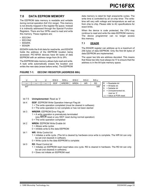
FIGURE 7-1: EECON1 REGISTER (ADDRESS 88h)<br />
<strong>PIC16F8X</strong><br />
data memory is rated for high erase/write cycles. The<br />
write time is controlled by an on-chip timer. The writetime<br />
will vary with voltage and temperature as well as<br />
from chip to chip. Please refer to AC specifications for<br />
exact limits.<br />
When the device is code protected, the CPU may<br />
continue to read and write the data <strong>EEPROM</strong> memory.<br />
The device programmer can no longer access<br />
this memory.<br />
7.1 EEADR<br />
The EEADR register can address up to a maximum of<br />
256 bytes of data <strong>EEPROM</strong>. Only the first 64 bytes of<br />
data <strong>EEPROM</strong> are implemented.<br />
The upper two bits are address decoded. This means<br />
that these two bits must always be '0' to ensure that the<br />
address is in the 64 byte memory space.<br />
U U U R/W-0 R/W-x R/W-0 R/S-0 R/S-x<br />
— — — EEIF WRERR WREN WR RD R = Readable bit<br />
bit7 bit0 W<br />
S<br />
= Writable bit<br />
= Settable bit<br />
U = Unimplemented bit,<br />
read as ‘0’<br />
- n = Value at POR reset<br />
bit 7:5 Unimplemented: Read as ’0’<br />
bit 4 EEIF: <strong>EEPROM</strong> Write Operation Interrupt Flag bit<br />
1 = The write operation completed (must be cleared in software)<br />
0 = The write operation is not complete or has not been started<br />
bit 3 WRERR: <strong>EEPROM</strong> Error Flag bit<br />
1 = A write operation is prematurely terminated<br />
(any MCLR reset or any WDT reset during normal operation)<br />
0 = The write operation completed<br />
bit 2 WREN: <strong>EEPROM</strong> Write Enable bit<br />
1 = Allows write cycles<br />
0 = Inhibits write to the data <strong>EEPROM</strong><br />
bit 1 WR: Write Control bit<br />
1 = initiates a write cycle. (The bit is cleared by hardware once write is complete. The WR bit can only<br />
be set (not cleared) in software.<br />
0 = Write cycle to the data <strong>EEPROM</strong> is complete<br />
bit 0 RD: Read Control bit<br />
1 = Initiates an <strong>EEPROM</strong> read (read takes one cycle. RD is cleared in hardware. The RD bit can only<br />
be set (not cleared) in software).<br />
0 = Does not initiate an <strong>EEPROM</strong> read<br />
© 1998 <strong>Microchip</strong> Technology Inc. DS30430C-page 33


