

PIC16F8X, 18-Pin FLASH/EEPROM 8-Bit MCU Data Sheet - Microchip
PIC16F8X, 18-Pin FLASH/EEPROM 8-Bit MCU Data Sheet - Microchip
PIC16F8X, 18-Pin FLASH/EEPROM 8-Bit MCU Data Sheet - Microchip

Create successful ePaper yourself
Turn your PDF publications into a flip-book with our unique Google optimized e-Paper software.
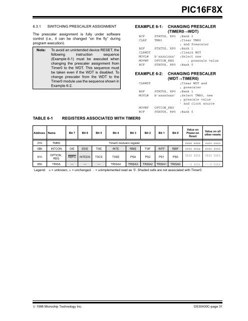
6.3.1 SWITCHING PRESCALER ASSIGNMENT<br />
The prescaler assignment is fully under software<br />
control (i.e., it can be changed “on the fly” during<br />
program execution).<br />
Note: To avoid an unintended device RESET, the<br />
following instruction sequence<br />
(Example 6-1) must be executed when<br />
changing the prescaler assignment from<br />
Timer0 to the WDT. This sequence must<br />
be taken even if the WDT is disabled. To<br />
change prescaler from the WDT to the<br />
Timer0 module use the sequence shown in<br />
Example 6-2.<br />
TABLE 6-1 REGISTERS ASSOCIATED WITH TIMER0<br />
<strong>PIC16F8X</strong><br />
EXAMPLE 6-1: CHANGING PRESCALER<br />
(TIMER0→WDT)<br />
BCF STATUS, RP0 ;Bank 0<br />
CLRF TMR0 ;Clear TMR0<br />
; and Prescaler<br />
BSF STATUS, RP0 ;Bank 1<br />
CLRWDT ;Clears WDT<br />
MOVLW b’xxxx1xxx’ ;Select new<br />
MOVWF OPTION_REG ; prescale value<br />
BCF STATUS, RP0 ;Bank 0<br />
EXAMPLE 6-2: CHANGING PRESCALER<br />
(WDT→TIMER0)<br />
CLRWDT ;Clear WDT and<br />
; prescaler<br />
BSF STATUS, RP0 ;Bank 1<br />
MOVLW b’xxxx0xxx’ ;Select TMR0, new<br />
; prescale value<br />
’ and clock source<br />
MOVWF OPTION_REG ;<br />
BCF STATUS, RP0 ;Bank 0<br />
Address Name <strong>Bit</strong> 7 <strong>Bit</strong> 6 <strong>Bit</strong> 5 <strong>Bit</strong> 4 <strong>Bit</strong> 3 <strong>Bit</strong> 2 <strong>Bit</strong> 1 <strong>Bit</strong> 0<br />
Value on<br />
Power-on<br />
Reset<br />
Value on all<br />
other resets<br />
01h TMR0 Timer0 module’s register xxxx xxxx uuuu uuuu<br />
0Bh INTCON GIE EEIE T0IE INTE RBIE T0IF INTF RBIF 0000 000x 0000 0000<br />
81h<br />
OPTION_<br />
REG<br />
RBPU INTEDG T0CS T0SE PSA PS2 PS1 PS0<br />
1111 1111 1111 1111<br />
85h TRISA — — — TRISA4 TRISA3 TRISA2 TRISA1 TRISA0 ---1 1111 ---1 1111<br />
Legend: x = unknown, u = unchanged. - = unimplemented read as ’0’. Shaded cells are not associated with Timer0.<br />
© 1998 <strong>Microchip</strong> Technology Inc. DS30430C-page 31


