

PIC16F8X, 18-Pin FLASH/EEPROM 8-Bit MCU Data Sheet - Microchip
PIC16F8X, 18-Pin FLASH/EEPROM 8-Bit MCU Data Sheet - Microchip
PIC16F8X, 18-Pin FLASH/EEPROM 8-Bit MCU Data Sheet - Microchip

Create successful ePaper yourself
Turn your PDF publications into a flip-book with our unique Google optimized e-Paper software.
9.0 INSTRUCTION SET SUMMARY<br />
Each PIC16CXX instruction is a 14-bit word divided<br />
into an OPCODE which specifies the instruction type<br />
and one or more operands which further specify the<br />
operation of the instruction. The PIC16CXX instruction<br />
set summary in Table 9-2 lists byte-oriented, bit-oriented,<br />
and literal and control operations. Table 9-1<br />
shows the opcode field descriptions.<br />
For byte-oriented instructions, ’f’ represents a file register<br />
designator and ’d’ represents a destination designator.<br />
The file register designator specifies which file<br />
register is to be used by the instruction.<br />
The destination designator specifies where the result of<br />
the operation is to be placed. If ’d’ is zero, the result is<br />
placed in the W register. If ’d’ is one, the result is placed<br />
in the file register specified in the instruction.<br />
For bit-oriented instructions, ’b’ represents a bit field<br />
designator which selects the number of the bit affected<br />
by the operation, while ’f’ represents the number of the<br />
file in which the bit is located.<br />
For literal and control operations, ’k’ represents an<br />
eight or eleven bit constant or literal value.<br />
TABLE 9-1 OPCODE FIELD<br />
DESCRIPTIONS<br />
Field Description<br />
f Register file address (0x00 to 0x7F)<br />
W Working register (accumulator)<br />
b <strong>Bit</strong> address within an 8-bit file register<br />
k Literal field, constant data or label<br />
x Don’t care location (= 0 or 1)<br />
The assembler will generate code with x = 0. It is the<br />
recommended form of use for compatibility with all<br />
<strong>Microchip</strong> software tools.<br />
d Destination select; d = 0: store result in W,<br />
d = 1: store result in file register f.<br />
Default is d = 1<br />
label Label name<br />
TOS Top of Stack<br />
PC Program Counter<br />
PCLATH Program Counter High Latch<br />
GIE Global Interrupt Enable bit<br />
WDT Watchdog Timer/Counter<br />
TO Time-out bit<br />
PD Power-down bit<br />
dest Destination either the W register or the specified<br />
register file location<br />
[ ] Options<br />
( ) Contents<br />
→ Assigned to<br />
< > Register bit field<br />
∈ In the set of<br />
italics User defined term (font is courier)<br />
<strong>PIC16F8X</strong><br />
The instruction set is highly orthogonal and is grouped<br />
into three basic categories:<br />
• Byte-oriented operations<br />
• <strong>Bit</strong>-oriented operations<br />
• Literal and control operations<br />
All instructions are executed within one single instruction<br />
cycle, unless a conditional test is true or the program<br />
counter is changed as a result of an instruction.<br />
In this case, the execution takes two instruction cycles<br />
with the second cycle executed as a NOP. One instruction<br />
cycle consists of four oscillator periods. Thus, for<br />
an oscillator frequency of 4 MHz, the normal instruction<br />
execution time is 1 μs. If a conditional test is true or the<br />
program counter is changed as a result of an instruction,<br />
the instruction execution time is 2 μs.<br />
Table 9-2 lists the instructions recognized by the<br />
MPASM assembler.<br />
Figure 9-1 shows the general formats that the instructions<br />
can have.<br />
Note: To maintain upward compatibility with<br />
future PIC16CXX products, do not use the<br />
OPTION and TRIS instructions.<br />
All examples use the following format to represent a<br />
hexadecimal number:<br />
0xhh<br />
where h signifies a hexadecimal digit.<br />
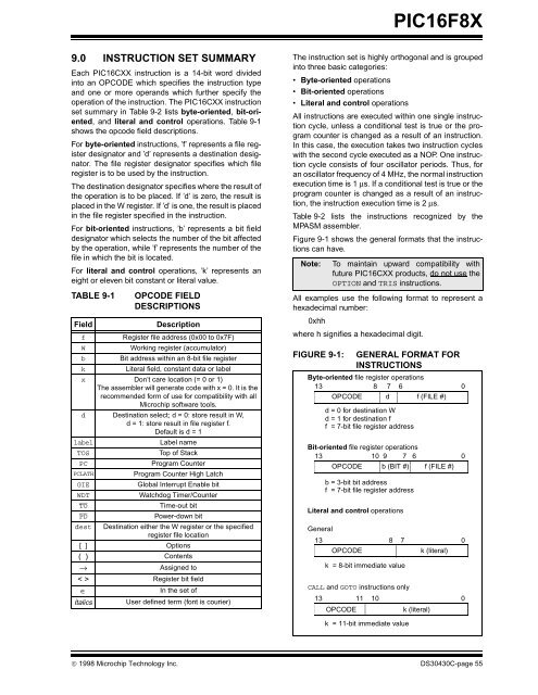
FIGURE 9-1: GENERAL FORMAT FOR<br />
INSTRUCTIONS<br />
Byte-oriented file register operations<br />
13 8 7 6 0<br />
OPCODE d f (FILE #)<br />
d = 0 for destination W<br />
d = 1 for destination f<br />
f = 7-bit file register address<br />
<strong>Bit</strong>-oriented file register operations<br />
13 10 9 7 6 0<br />
OPCODE b (BIT #) f (FILE #)<br />
b = 3-bit bit address<br />
f = 7-bit file register address<br />
Literal and control operations<br />
General<br />
13 8 7 0<br />
OPCODE k (literal)<br />
k = 8-bit immediate value<br />
CALL and GOTO instructions only<br />
13 11 10 0<br />
OPCODE k (literal)<br />
k = 11-bit immediate value<br />
© 1998 <strong>Microchip</strong> Technology Inc. DS30430C-page 55


