

PIC16F8X, 18-Pin FLASH/EEPROM 8-Bit MCU Data Sheet - Microchip
PIC16F8X, 18-Pin FLASH/EEPROM 8-Bit MCU Data Sheet - Microchip
PIC16F8X, 18-Pin FLASH/EEPROM 8-Bit MCU Data Sheet - Microchip

You also want an ePaper? Increase the reach of your titles
YUMPU automatically turns print PDFs into web optimized ePapers that Google loves.
<strong>PIC16F8X</strong><br />
7.2 EECON1 and EECON2 Registers<br />
EECON1 is the control register with five low order bits<br />
physically implemented. The upper-three bits are nonexistent<br />
and read as ’0’s.<br />
Control bits RD and WR initiate read and write,<br />
respectively. These bits cannot be cleared, only set, in<br />
software. They are cleared in hardware at completion<br />
of the read or write operation. The inability to clear the<br />
WR bit in software prevents the accidental, premature<br />
termination of a write operation.<br />
The WREN bit, when set, will allow a write operation.<br />
On power-up, the WREN bit is clear. The WRERR bit is<br />
set when a write operation is interrupted by a MCLR<br />
reset or a WDT time-out reset during normal operation.<br />
In these situations, following reset, the user can check<br />
the WRERR bit and rewrite the location. The data and<br />
address will be unchanged in the EEDATA and<br />
EEADR registers.<br />
Interrupt flag bit EEIF is set when write is complete. It<br />
must be cleared in software.<br />
EECON2 is not a physical register. Reading EECON2<br />
will read all ’0’s. The EECON2 register is used<br />
exclusively in the <strong>Data</strong> <strong>EEPROM</strong> write sequence.<br />
7.3 Reading the <strong>EEPROM</strong> <strong>Data</strong> Memory<br />
To read a data memory location, the user must write the<br />
address to the EEADR register and then set control bit<br />
RD (EECON1). The data is available, in the very<br />
next cycle, in the EEDATA register; therefore it can be<br />
read in the next instruction. EEDATA will hold this value<br />
until another read or until it is written to by the user<br />
(during a write operation).<br />
EXAMPLE 7-1: DATA <strong>EEPROM</strong> READ<br />
BCF STATUS, RP0 ; Bank 0<br />
MOVLW CONFIG_ADDR ;<br />
MOVWF EEADR ; Address to read<br />
BSF STATUS, RP0 ; Bank 1<br />
BSF EECON1, RD ; EE Read<br />
BCF STATUS, RP0 ; Bank 0<br />
MOVF EEDATA, W ; W = EEDATA<br />
7.4 Writing to the <strong>EEPROM</strong> <strong>Data</strong> Memory<br />
To write an <strong>EEPROM</strong> data location, the user must first<br />
write the address to the EEADR register and the data<br />
to the EEDATA register. Then the user must follow a<br />
specific sequence to initiate the write for each byte.<br />
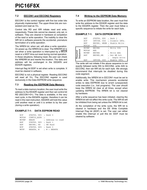
EXAMPLE 7-1: DATA <strong>EEPROM</strong> WRITE<br />
BSF STATUS, RP0 ; Bank 1<br />
BCF INTCON, GIE ; Disable INTs.<br />
BSF EECON1, WREN ; Enable Write<br />
MOVLW 55h ;<br />
MOVWF EECON2 ; Write 55h<br />
MOVLW AAh ;<br />
MOVWF EECON2 ; Write AAh<br />
BSF EECON1,WR ; Set WR bit<br />
; begin write<br />
BSF INTCON, GIE ; Enable INTs.<br />
The write will not initiate if the above sequence is not<br />
exactly followed (write 55h to EECON2, write AAh to<br />
EECON2, then set WR bit) for each byte. We strongly<br />
recommend that interrupts be disabled during this<br />
code segment.<br />
Additionally, the WREN bit in EECON1 must be set to<br />
enable write. This mechanism prevents accidental<br />
writes to data <strong>EEPROM</strong> due to errant (unexpected)<br />
code execution (i.e., lost programs). The user should<br />
keep the WREN bit clear at all times, except when<br />
updating <strong>EEPROM</strong>. The WREN bit is not cleared<br />
by hardware<br />
After a write sequence has been initiated, clearing the<br />
WREN bit will not affect this write cycle. The WR bit will<br />
be inhibited from being set unless the WREN bit is set.<br />
At the completion of the write cycle, the WR bit is<br />
cleared in hardware and the EE Write Complete<br />
Interrupt Flag bit (EEIF) is set. The user can either<br />
enable this interrupt or poll this bit. EEIF must be<br />
cleared by software.<br />
DS30430C-page 34 © 1998 <strong>Microchip</strong> Technology Inc.<br />
Required<br />
Sequence


