

PIC16F8X, 18-Pin FLASH/EEPROM 8-Bit MCU Data Sheet - Microchip
PIC16F8X, 18-Pin FLASH/EEPROM 8-Bit MCU Data Sheet - Microchip
PIC16F8X, 18-Pin FLASH/EEPROM 8-Bit MCU Data Sheet - Microchip

Create successful ePaper yourself
Turn your PDF publications into a flip-book with our unique Google optimized e-Paper software.
5.0 I/O PORTS<br />
The <strong>PIC16F8X</strong> has two ports, PORTA and PORTB.<br />
Some port pins are multiplexed with an alternate function<br />
for other features on the device.<br />
5.1 PORTA and TRISA Registers<br />
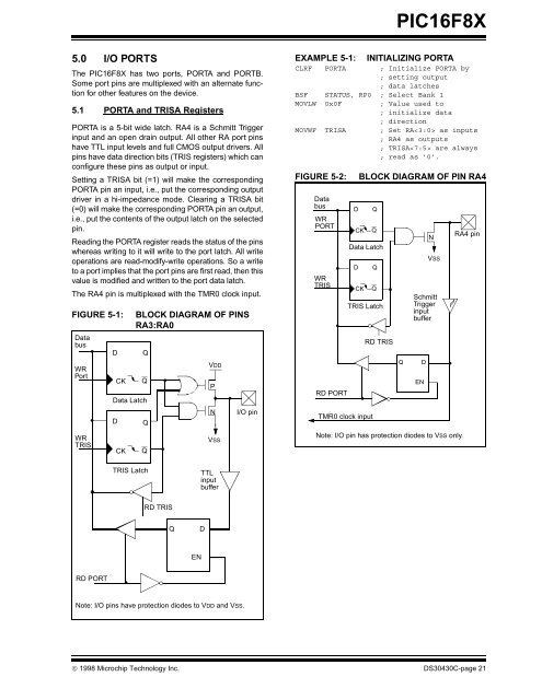
PORTA is a 5-bit wide latch. RA4 is a Schmitt Trigger<br />
input and an open drain output. All other RA port pins<br />
have TTL input levels and full CMOS output drivers. All<br />
pins have data direction bits (TRIS registers) which can<br />
configure these pins as output or input.<br />
Setting a TRISA bit (=1) will make the corresponding<br />
PORTA pin an input, i.e., put the corresponding output<br />
driver in a hi-impedance mode. Clearing a TRISA bit<br />
(=0) will make the corresponding PORTA pin an output,<br />
i.e., put the contents of the output latch on the selected<br />
pin.<br />
Reading the PORTA register reads the status of the pins<br />
whereas writing to it will write to the port latch. All write<br />
operations are read-modify-write operations. So a write<br />
to a port implies that the port pins are first read, then this<br />
value is modified and written to the port data latch.<br />
The RA4 pin is multiplexed with the TMR0 clock input.<br />
FIGURE 5-1: BLOCK DIAGRAM OF PINS<br />
RA3:RA0<br />
<strong>Data</strong><br />
bus<br />
WR<br />
Port<br />
WR<br />
TRIS<br />
RD PORT<br />
D<br />
D<br />
CK<br />
CK<br />
Q<br />
Q<br />
<strong>Data</strong> Latch<br />
Q<br />
Q<br />
TRIS Latch<br />
RD TRIS<br />
Q D<br />
EN<br />
VDD<br />
Note: I/O pins have protection diodes to VDD and VSS.<br />
P<br />
N<br />
VSS<br />
TTL<br />
input<br />
buffer<br />
I/O pin<br />
<strong>PIC16F8X</strong><br />
EXAMPLE 5-1: INITIALIZING PORTA<br />
CLRF PORTA ; Initialize PORTA by<br />
; setting output<br />
; data latches<br />
BSF STATUS, RP0 ; Select Bank 1<br />
MOVLW 0x0F ; Value used to<br />
; initialize data<br />
; direction<br />
MOVWF TRISA ; Set RA as inputs<br />
; RA4 as outputs<br />
; TRISA are always<br />
; read as ’0’.<br />
FIGURE 5-2: BLOCK DIAGRAM OF PIN RA4<br />
<strong>Data</strong><br />
bus<br />
WR<br />
PORT<br />
© 1998 <strong>Microchip</strong> Technology Inc. DS30430C-page 21<br />
WR<br />
TRIS<br />
RD PORT<br />
D<br />
CK<br />
<strong>Data</strong> Latch<br />
D<br />
CK<br />
TRIS Latch<br />
TMR0 clock input<br />
Q<br />
Q<br />
Q<br />
Q<br />
RD TRIS<br />
N<br />
VSS<br />
Schmitt<br />
Trigger<br />
input<br />
buffer<br />
Q D<br />
EN<br />
Note: I/O pin has protection diodes to VSS only.<br />
RA4 pin


