- Page 1 and 2:
Power and Energy Management of Mult
- Page 3 and 4:
Acknowledgements This journey would
- Page 5 and 6:
Nomenclature Notation Description U
- Page 7 and 8:
Abbreviations Batt (batt) Battery D
- Page 9 and 10:
Contents 3.19 Ultracapacitor Power
- Page 11 and 12:
List of Figures List of Figures Fig
- Page 13 and 14:
List of Figures Figure 6.3 Power de
- Page 15 and 16:
Chapter 1 CHAPTER 1 INTRODUCTION
- Page 17 and 18:
Chapter 1 more than a century since
- Page 19 and 20:
Chapter 1 EV Charge Depleting Energ
- Page 21 and 22:
Chapter 1 1745 Invention of the cap
- Page 23 and 24:
Chapter 1 generated, and split betw
- Page 25 and 26:
Chapter 1 In the past, many researc
- Page 27 and 28:
Chapter 1 1.7 Contributions This th
- Page 29 and 30:
Chapter 1 7. As the hybridisation o
- Page 31 and 32:
Chapter 1 1.9 Publications The foll
- Page 33 and 34:
Chapter 2 CHAPTER 2 LITERATURE REVI
- Page 35 and 36:
Chapter 2 in the area or power and
- Page 37 and 38:
Chapter 2 Power Load Demand Time Po
- Page 39 and 40:
Chapter 2 previewed information abo
- Page 41 and 42:
Chapter 2 generally used. They are,
- Page 43 and 44:
Chapter 2 the large capacitive phen
- Page 45 and 46:
Chapter 2 manufacturer. Throughout
- Page 47 and 48:
Chapter 2 energy density attributes
- Page 49 and 50:
Chapter 2 experimentally verified a
- Page 51 and 52:
Chapter 2 Propulsion Load Batteries
- Page 53 and 54:
Chapter 2 system. They compared the
- Page 55 and 56:
Chapter 2 2.6 Ultracapacitor augmen
- Page 57 and 58:
Chapter 2 2.8 Observations and Hypo
- Page 59 and 60:
Chapter 2 Literature concerning veh
- Page 61 and 62:
Chapter 2 philosophical concepts fo
- Page 63 and 64:
Chapter 3 3.1 EV Battery Systems In
- Page 65 and 66:
Chapter 3 The equivalent circuit lo
- Page 67 and 68:
Chapter 3 merits, some of these tec
- Page 69 and 70:
Chapter 3 where 1Ah = 3600C. The Ah
- Page 71 and 72:
Chapter 3 same state of charge. As
- Page 73 and 74:
Chapter 3 The state of discharge (S
- Page 75 and 76:
Chapter 3 provided by the battery m
- Page 77 and 78:
Chapter 3 Figure 3.5 illustrates an
- Page 79 and 80:
Chapter 3 where Voc[SoC] and Ri[SoC
- Page 81 and 82:
Chapter 3 Power(Watt) 4000 3500 300
- Page 83 and 84:
Chapter 3 Batt Voltage (V) Charging
- Page 85 and 86:
Chapter 3 Voc Voc Ri Ri R chg R chg
- Page 87 and 88:
Chapter 3 Description [Unit] Parame
- Page 89 and 90:
Chapter 3 3.17 Ultracapacitors Ultr
- Page 91 and 92:
Chapter 3 voltage on charge and a d
- Page 93 and 94:
Chapter 3 As with the battery model
- Page 95 and 96:
Chapter 3 The energy capacity, E of
- Page 97 and 98:
Chapter 3 3.20 Ultracapacitors in s
- Page 99 and 100:
Chapter 3 Voltage (V) Time (s) 92 p
- Page 101 and 102:
Chapter 3 3.21 Hybridisation of Bat
- Page 103 and 104:
Chapter 3 83.50 50.00 Current (A) 0
- Page 105 and 106:
Chapter 3 In section 3.11, it was s
- Page 107 and 108:
Chapter 4 4.1 Vehicle Longitudinal
- Page 109 and 110:
Chapter 4 where sgn[vxT] is a the s
- Page 111 and 112:
Chapter 4 P Load dP Load /dt > 0 P
- Page 113 and 114:
Chapter 4 braking energy. Regenerat
- Page 115 and 116:
Chapter 4 Angular Velocity (rad/s)
- Page 117 and 118:
Chapter 4 electrical terminal power
- Page 119 and 120:
Chapter 4 112 Type 1 -Energy Sytem
- Page 121 and 122:
Chapter 4 Battery Power (W) Profile
- Page 123 and 124:
Chapter 4 Energy (J) CASE 2 Battery
- Page 125 and 126:
Chapter 4 Battery Power (W) Profile
- Page 127 and 128:
Chapter 4 Energy (J) CASE 3 Battery
- Page 129 and 130:
Chapter 4 Energy (J) Energy (J) DIS
- Page 131 and 132:
Chapter 4 occur more frequently bef
- Page 133 and 134:
Chapter 5 CHAPTER 5 THE MANAGEMENT
- Page 135 and 136:
Chapter 5 Under the directives and
- Page 137 and 138:
Chapter 5 Hierarchy Mid-Level Low-L
- Page 139 and 140:
Chapter 5 While the breadth of the
- Page 141 and 142:
Chapter 5 The complete modular stru
- Page 143 and 144:
Chapter 5 conceive and implement. T
- Page 145 and 146:
Chapter 5 where, P req is the reque
- Page 147 and 148:
Chapter 5 Max Velocity Mode [Run,Id
- Page 149 and 150:
Chapter 5 decision epoch window (
- Page 151 and 152:
Chapter 5 P uc max Power 0 ∆PMS t
- Page 153 and 154:
Chapter 5 (W) (W) (W) Figure 5.11 L
- Page 155 and 156:
Chapter 5 An important difference w
- Page 157 and 158:
Chapter 5 IF x1 is Ai1 AND x2 is Ai
- Page 159 and 160:
Chapter 5 In this strategy, only P
- Page 161 and 162: Chapter 5 to a fixed PMS policy. As
- Page 163 and 164: Chapter 5 P DCBUS 000 dP/dt >0 P>0
- Page 165 and 166: Chapter 5 For a PES with two refere
- Page 167 and 168: Chapter 5 Thus the connection matri
- Page 169 and 170: Chapter 5 5.12 Summary The foundati
- Page 171 and 172: Chapter 6 6.1 The experimental vehi
- Page 173 and 174: Chapter 6 Power (W) / Energy (Wh) P
- Page 175 and 176: Chapter 6 System Voltage Measuremen
- Page 177 and 178: Chapter 6 Velocity (km/h) 60 50 40
- Page 179 and 180: Chapter 7 CHAPTER 7 IMPLEMENTATION
- Page 181 and 182: Chapter 7 Battery C batt L batt T1
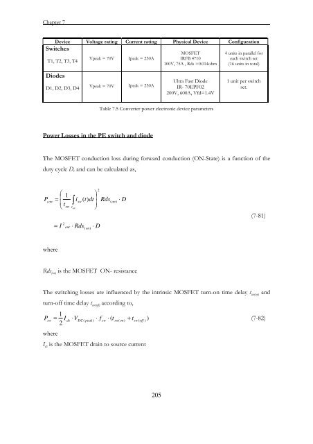
- Page 183 and 184: Chapter 7 Parameter Notation Values
- Page 185 and 186: Chapter 7 During the conduction per
- Page 187 and 188: Chapter 7 Design and sizing of the
- Page 189 and 190: Chapter 7 7.6 Battery Buck Mode - C
- Page 191 and 192: Chapter 7 L batt = ( Vout )( 1 DT1
- Page 193 and 194: Chapter 7 7.7 Ultracapacitor Boost
- Page 195 and 196: Chapter 7 1 ⇒ ⋅ 0. 67 20kHz whi
- Page 197 and 198: Chapter 7 L uc Vout DT 4 ( 1− DT
- Page 199 and 200: Chapter 7 20 D T 3 min = = 0. 31 (7
- Page 201 and 202: Chapter 7 A similar value for the i
- Page 203 and 204: Chapter 7 the inductor current (20k
- Page 205 and 206: Chapter 7 The maximum current that
- Page 207 and 208: Chapter 7 According to Arnet and Ha
- Page 209 and 210: Chapter 7 The second dimensioning f
- Page 211: Chapter 7 + - 2200uF Figure 7.11 Sc
- Page 215 and 216: Chapter 8 CHAPTER 8 EXPERIMENTS AND
- Page 217 and 218: Chapter 8 Segment 1 Battery Current
- Page 219 and 220: Chapter 8 Discussion: From the 600-
- Page 221 and 222: Chapter 8 Results: Figure 8.5 shows
- Page 223 and 224: Chapter 8 Discussion: The top graph
- Page 225 and 226: Chapter 8 8.3. Experiment 3: Power
- Page 227 and 228: Chapter 8 Test Segment 1 Power (W)
- Page 229 and 230: Chapter 8 Test Segment 3 Power (W)
- Page 231 and 232: Chapter 8 Discussion: Results of th
- Page 233 and 234: Chapter 8 Battery Voltage (V) Batte
- Page 235 and 236: Chapter 8 8.4. PES Type Test Purpos
- Page 237 and 238: Chapter 8 Current (A) Boolean PWM s
- Page 239 and 240: Chapter 9 CHAPTER 9 CONCLUSIONS AND
- Page 241 and 242: Chapter 9 The M-PEMS framework does
- Page 243 and 244: Chapter 9 between sources. Doing so
- Page 245 and 246: Chapter 9 to be included in measuri
- Page 247 and 248: References [15] R. H. Staunton, C.
- Page 249 and 250: References [43] B. E. Conway, Elect
- Page 251 and 252: References [73] A. Drolia, P. Jose,
- Page 253 and 254: References [101] E. Surewaard, E. K
- Page 255 and 256: Appendices Appendix A: Schematics A
- Page 257 and 258: 1 2 3 4 5 6 7 A ID TB1 Fuse Fuse Fu
- Page 259 and 260: 1 2 3 4 5 6 7 A Bus Bars φ = φ =
- Page 261 and 262: 1 2 3 4 5 6 7 A ID A B D B C D E F
- Page 263 and 264:
1 2 3 4 5 6 7 A ID L batt L UC K1 B
- Page 265 and 266:
1 2 3 4 5 6 7 A ID START STOP START
- Page 267 and 268:
1 2 3 4 5 6 7 A ID B C D E F G H I
- Page 269 and 270:
1 2 3 4 5 6 7 A ID START STOP START
- Page 271 and 272:
Minimum Duty Cycle Maximum Duty Cyc
- Page 273 and 274:
Type Test- 03 Type testing of the g
- Page 275 and 276:
Power, interfacing and sub control