Enabler II-G Assiste GPS Integration Guide - Farnell
Enabler II-G Assiste GPS Integration Guide - Farnell
Enabler II-G Assiste GPS Integration Guide - Farnell

Create successful ePaper yourself
Turn your PDF publications into a flip-book with our unique Google optimized e-Paper software.
Enfora <strong>Enabler</strong> <strong>II</strong>I-G<br />
Modem <strong>Integration</strong> <strong>Guide</strong><br />
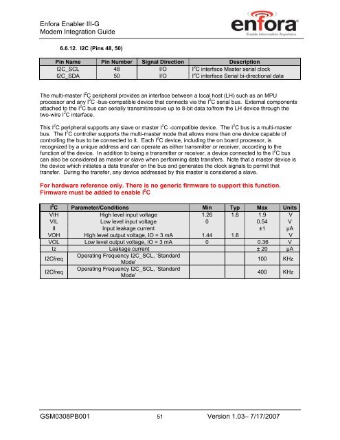
6.6.12. I2C (Pins 48, 50)<br />
Pin Name Pin Number Signal Direction Description<br />
I2C_SCL 48 I/O I 2 C interface Master serial clock<br />
I2C_SDA 50 I/O I 2 C interface Serial bi-directional data<br />
The multi-master I 2 C peripheral provides an interface between a local host (LH) such as an MPU<br />
processor and any I 2 C -bus-compatible device that connects via the I 2 C serial bus. External components<br />
attached to the I 2 C bus can serially transmit/receive up to 8-bit data to/from the LH device through the<br />
two-wire I 2 C interface.<br />
2 2<br />
This I C peripheral supports any slave or master I C -compatible device. The I 2 C bus is a multi-master<br />
bus. The I 2 C controller supports the multi-master mode that allows more than one device capable of<br />
controlling the bus to be connected to it. Each I 2 C device, including the on board processor, is<br />
recognized by a unique address and can operate as either transmitter or receiver, according to the<br />
function of the device. In addition to being a transmitter or receiver, a device connected to the I 2 C bus<br />
can also be considered as master or slave when performing data transfers. Note that a master device is<br />
the device which initiates a data transfer on the bus and generates the clock signals to permit that<br />
transfer. During the transfer, any device addressed by this master is considered a slave.<br />
For hardware reference only. There is no generic firmware to support this function.<br />
Firmware must be added to enable I 2 C<br />
I 2 C Parameter/Conditions Min Typ Max Units<br />
VIH High level input voltage 1.26 1.8 1.9 V<br />
VIL Low level input voltage 0 0.54 V<br />
<strong>II</strong> Input leakage current ±1 μA<br />
VOH High level output voltage, IO = 3 mA 1.44 1.8 V<br />
VOL Low level output voltage, IO = 3 mA 0 0.36 V<br />
Iz Leakage current ± 20 μA<br />
I2Cfreq<br />
Operating Frequency I2C_SCL, ‘Standard<br />
100 KHz<br />
I2Cfreq<br />
Mode’<br />
Operating Frequency I2C_SCL, ‘Standard<br />
Mode’<br />
400 KHz<br />
GSM0308PB001 51 Version 1.03– 7/17/2007