

ADV7174/ADV7179 Chip Scale PAL/NTSC Video ... - Analog Devices
ADV7174/ADV7179 Chip Scale PAL/NTSC Video ... - Analog Devices
ADV7174/ADV7179 Chip Scale PAL/NTSC Video ... - Analog Devices

Create successful ePaper yourself
Turn your PDF publications into a flip-book with our unique Google optimized e-Paper software.
FEATURES<br />
ITU-R1 BT601/BT656 YCrCb to <strong>PAL</strong>/<strong>NTSC</strong> video encoder<br />
High quality 10-bit video DACs<br />
SSAF (super sub-alias filter)<br />
Advanced power management features<br />
CGMS (copy generation management system)<br />
WSS (wide screen signaling)<br />
<strong>NTSC</strong> M, <strong>PAL</strong> N2 , <strong>PAL</strong> B/D/G/H/I, <strong>PAL</strong>-M3 , <strong>PAL</strong> 60<br />
Single 27 MHz clock required (×2 oversampling)<br />
Macrovision 7.1 (<strong>ADV7174</strong> only)<br />
80 dB video SNR<br />
32-bit direct digital synthesizer for color subcarrier<br />
Multistandard video output support:<br />
Composite (CVBS)<br />
Component S-video (Y/C)<br />
<strong>Video</strong> input data port supports:<br />
CCIR-656 4:2:2 8-bit parallel input format<br />
Programmable simultaneous composite and S-video or RGB<br />
(SCART)/YPbPr video outputs<br />
Programmable luma filters low-pass [<strong>PAL</strong>/<strong>NTSC</strong>] notch,<br />
extended SSAF, CIF, and QCIF<br />
Programmable chroma filters (low-pass [0.65 MHz, 1.0 MHz,<br />
1.2 MHz, and 2.0 MHz], CIF, and QCIF)<br />
Programmable VBI (vertical blanking interval)<br />
V AA<br />
RESET<br />
COLOR<br />
DATA<br />
P7–P0<br />
HSYNC<br />
FIELD/VSYNC<br />
BLANK<br />
POWER<br />
MANAGEMENT<br />
CONTROL<br />
(SLEEP MODE)<br />
4:2:2 TO<br />
4:4:4<br />
INTER-<br />
POLATOR<br />
8<br />
8<br />
8<br />
VIDEO TIMING<br />
GENERATOR<br />
Rev. B<br />
Information furnished by <strong>Analog</strong> <strong>Devices</strong> is believed to be accurate and reliable. However, no<br />
responsibility is assumed by <strong>Analog</strong> <strong>Devices</strong> for its use, nor for any infringements of patents or other<br />
rights of third parties that may result from its use. Specifications subject to change without notice. No<br />
license is granted by implication or otherwise under any patent or patent rights of <strong>Analog</strong> <strong>Devices</strong>.<br />
Trademarks and registered trademarks are the property of their respective owners.<br />
V<br />
8<br />
8<br />
I 2 C MPU PORT<br />
<strong>Chip</strong> <strong>Scale</strong> <strong>PAL</strong>/<strong>NTSC</strong> <strong>Video</strong> Encoder with<br />
Advanced Power Management<br />
<strong>ADV7174</strong>/<strong>ADV7179</strong><br />
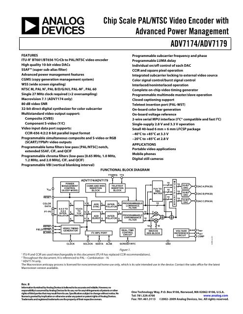
FUNCTIONAL BLOCK DIAGRAM<br />
TTXREQ TTX<br />
<strong>ADV7174</strong>/<strong>ADV7179</strong><br />
CGMS AND WSS TELETEXT<br />
INSERTION INSERTION<br />
BLOCK<br />
BLOCK<br />
8<br />
REAL-TIME<br />
CONTROL<br />
CIRCUIT<br />
Programmable subcarrier frequency and phase<br />
Programmable LUMA delay<br />
Individual on/off control of each DAC<br />
CCIR and square pixel operation<br />
Integrated subcarrier locking to external video source<br />
Color signal control/burst signal control<br />
Interlaced/noninterlaced operation<br />
Complete on-chip video timing generator<br />
Programmable multimode master/slave operation<br />
Closed captioning support<br />
Teletext insertion port (<strong>PAL</strong>-WST)<br />
On-board color bar generation<br />
On-board voltage reference<br />
2-wire serial MPU interface (I2C® compatible and fast I2C) Single-supply 2.8 V and 3.3 V operation<br />
Small 40-lead 6 mm × 6 mm LFCSP package<br />
−40°C to +85°C at 3.3 V<br />
−20°C to +85°C at 2.8 V<br />
APPLICATIONS<br />
Portable video applications<br />
Mobile phones<br />
Digital still cameras<br />
10<br />
YUV TO<br />
RBG<br />
MATRIX<br />
YCrCb<br />
Y 8<br />
ADD<br />
SYNC<br />
9 INTER- 9<br />
POLATOR<br />
PROGRAMMABLE<br />
LUMINANCE<br />
FILTER<br />
10<br />
TO<br />
YUV<br />
MATRIX<br />
U 8 8<br />
8<br />
10 U<br />
ADD<br />
BURST<br />
INTER-<br />
POLATOR<br />
PROGRAMMABLE<br />
CHROMINANCE<br />
FILTER<br />
10 10<br />
SIN/COS<br />
DDS BLOCK<br />
CLOCK SCLOCK SDATA ALSB SCRESET/RTC<br />
GND<br />
Figure 1.<br />
V<br />
10<br />
10<br />
10<br />
M<br />
U L<br />
T<br />
I<br />
P<br />
L<br />
E<br />
X<br />
E<br />
R<br />
10<br />
10<br />
10<br />
10-BIT<br />
DAC<br />
10-BIT<br />
DAC<br />
10-BIT<br />
DAC<br />
VOLTAGE<br />
REFERENCE<br />
CIRCUIT<br />
DACA(PIN29)<br />
DACB(PIN28)<br />
DACC(PIN24)<br />
1 ITU-R and CCIR are used interchangeably in this document (ITU-R has replaced CCIR recommendations).<br />
2 Throughout the document, N is referenced to <strong>PAL</strong> – Combination – N.<br />
3 <strong>ADV7174</strong> only.<br />
The Macrovision anticopy process is licensed for noncommercial home use only, which is its sole intended use in the device. Contact the sales office for the latest<br />
Macrovision version available.<br />
V REF<br />
R SET<br />
COMP<br />
One Technology Way, P.O. Box 9106, Norwood, MA 02062-9106, U.S.A.<br />
Tel: 781.329.4700 www.analog.com<br />
Fax: 781.461.3113 ©2002–2009 <strong>Analog</strong> <strong>Devices</strong>, Inc. All rights reserved.<br />
02980-A-001
<strong>ADV7174</strong>/<strong>ADV7179</strong><br />
TABLE OF CONTENTS<br />
Specifications ..................................................................................... 4<br />
2.8 V Specifications ...................................................................... 4<br />
2.8 V Timing Specifications ........................................................ 5<br />
3.3 V Specifications ...................................................................... 6<br />
3.3 V Timing Specifications ........................................................ 7<br />
Absolute Maximum Ratings ............................................................ 9<br />
ESD Caution .................................................................................. 9<br />
Pin Configuration and Function Descriptions ........................... 10<br />
General Description ....................................................................... 11<br />
Data Path Description ................................................................ 11<br />
Internal Filter Response ............................................................. 11<br />
Typical Performance Characteristics ........................................... 13<br />
Features ............................................................................................ 16<br />
Color Bar Generation ................................................................ 16<br />
Square Pixel Mode ...................................................................... 16<br />
Color Signal Control .................................................................. 16<br />
Burst Signal Control ................................................................... 16<br />
<strong>NTSC</strong> Pedestal Control ............................................................. 16<br />
Pixel Timing Description .......................................................... 16<br />
8-Bit YCrCb Mode ................................................................. 16<br />
Subcarrier Reset .......................................................................... 16<br />
Real-Time Control ..................................................................... 16<br />
<strong>Video</strong> Timing Description .................................................... 16<br />
Vertical Blanking Data Insertion.......................................... 17<br />
Mode 0 (CCIR-656): Slave Option ....................................... 17<br />
Mode 0 (CCIR-656): Master Option ................................... 17<br />
Mode 1: Slave Option HSYNC, BLANK, FIELD ............... 20<br />
Mode 1: Master Option HSYNC, BLANK, FIELD ............ 21<br />
Mode 2: Slave Option HSYNC, VSYNC, BLANK ............. 22<br />
Mode 2: Master Option HSYNC, VSYNC, BLANK .......... 23<br />
Rev. B | Page 2 of 52<br />
Mode 3: Master/Slave Option HSYNC, BLANK, FIELD . 24<br />
Power-On Reset .......................................................................... 25<br />
SCH Phase Mode ........................................................................ 25<br />
MPU Port Description ............................................................... 25<br />
Register Accesses ........................................................................ 26<br />
Register Programming ................................................................... 27<br />
Subaddress Register (SR7–SR0) ............................................... 27<br />
Register Select (SR5–SR0) ......................................................... 27<br />
Mode Register 1 (MR1) ............................................................. 29<br />
Mode Register 2 (MR2) ............................................................. 30<br />
Mode Register 3 (MR3) ............................................................. 31<br />
Mode Register 4 (MR4) ............................................................. 32<br />
Timing Mode Register 0 (TR0) ................................................ 33<br />
Timing Mode Register 1 (TR1) ................................................ 34<br />
Subcarrier Frequency Registers 3–0 ........................................ 35<br />
Subcarrier Phase Register .......................................................... 35<br />
Closed Captioning Even Field Data Registers 1–0 ................ 35<br />
Closed Captioning Odd Field Data Registers 1–0 ................. 36<br />
<strong>NTSC</strong> Pedestal/<strong>PAL</strong> Teletext Control Registers 3–0 ............. 36<br />
Teletext Request Control Register (TC07) .............................. 37<br />
CGMS_WSS Register 0 (C/W0) ............................................... 37<br />
CGMS_WSS Register 1 (C/W1) ............................................... 38<br />
CGMS_WSS Register 2 (C/W2) ............................................... 38<br />
Appendix 1—Board Design and Layout Considerations .......... 39<br />
Ground Planes ............................................................................ 39<br />
Power Planes ............................................................................... 39<br />
Supply Decoupling ..................................................................... 40<br />
Digital Signal Interconnect ....................................................... 40<br />
<strong>Analog</strong> Signal Interconnect....................................................... 40<br />
Appendix 2—Closed Captioning ................................................. 41
Appendix 3—Copy Generation Management System (CGMS)<br />
............................................................................................................ 42<br />
Function of CGMS Bits .............................................................. 42<br />
Appendix 4—Wide Screen Signaling (WSS) ............................... 43<br />
Function of WSS Bits .................................................................. 43<br />
Appendix 5—Teletext ..................................................................... 44<br />
Teletext Insertion......................................................................... 44<br />
Teletext Protocol .......................................................................... 44<br />
Appendix 6—Waveforms ............................................................... 45<br />
REVISION HISTORY<br />
4/09—Rev. A to Rev. B<br />
Changes to Power-On Reset Section ............................................ 25<br />
Changes to Figure 55 ...................................................................... 40<br />
Changes to Figure 69, Figure 70, and Figure 72 .......................... 47<br />
Changes to Figure 81 Caption ....................................................... 52<br />
Changes to Ordering Guide ........................................................... 52<br />
2/04—Changed from Rev. 0 to Rev A.<br />
Added 2.8 V Version .......................................................... Universal<br />
Format Updated.................................................................. Universal<br />
Device Currents Updated on 3.3 V Specification .......... Universal<br />
Added new Table 1 and renumbered Subsequent Tables ............. 4<br />
Added new Table 2 and Renumbered Subsequent Tables ........... 5<br />
Change to Figure 54 ........................................................................ 38<br />
Change to Figure 55 ........................................................................ 39<br />
Change to Figure 79 ........................................................................ 48<br />
Changed Ordering Guide Temperature Specifications .............. 52<br />
Updated Outline Dimensions ........................................................ 52<br />
10/02—Revision 0: Initial Version<br />
Rev. B | Page 3 of 52<br />
<strong>ADV7174</strong>/<strong>ADV7179</strong><br />
<strong>NTSC</strong> Waveforms (with Pedestal) ............................................ 45<br />
<strong>NTSC</strong> Waveforms (without Pedestal) ...................................... 46<br />
<strong>PAL</strong> Waveforms ........................................................................... 47<br />
Pb Pr Waveforms ......................................................................... 48<br />
Appendix 7—Optional Output Filter ........................................... 49<br />
Appendix 8—Recommended Register Values............................. 50<br />
Outline Dimensions ........................................................................ 52<br />
Ordering Guide ........................................................................... 52
<strong>ADV7174</strong>/<strong>ADV7179</strong><br />
SPECIFICATIONS<br />
2.8 V SPECIFICATIONS<br />
VAA = 2.8 V, VREF = 1.235 V, RSET = 150 Ω. All specifications TMIN to TMAX 1 , unless otherwise noted.<br />
Table 1.<br />
Parameter Conditions1 STATIC PERFORMANCE<br />
Min Typ Max Unit<br />
2<br />
Resolution (Each DAC)<br />
Accuracy (Each DAC)<br />
10 Bits<br />
Integral Nonlinearity RSET = 300 Ω ±3.0 LSB<br />
Differential Nonlinearity<br />
DIGITAL INPUTS<br />
Guaranteed monotonic ±1 LSB<br />
2<br />
Input High Voltage, VINH 1.6 V<br />
Input Low Voltage, VINL 0.7 V<br />
Input Current, IIN VIN = 0.4 V or 2.4 V ±1 μA<br />
Input Capacitance, CIN<br />
DIGITAL OUTPUTS<br />
10 pF<br />
2<br />
Output High Voltage, VOH ISOURCE = 400 μA 2.4 V<br />
Output Low Voltage, VOL ISINK = 3.2 mA 0.4 V<br />
Three-State Leakage Current 10 μA<br />
Three-State Output Capacitance<br />
ANALOG OUTPUTS<br />
10 pF<br />
2<br />
Output Current 3 RSET = 150 Ω, RL = 37.5 Ω 33 34.7 37 mA<br />
DAC-to-DAC Matching 2.0 %<br />
Output Compliance, VOC 0 1.4 V<br />
Output Impedance, ROUT 30 kΩ<br />
Output Capacitance, COUT<br />
2, 4<br />
POWER REQUIREMENTS<br />
IOUT = 0 mA 30 pF<br />
VAA<br />
Normal Power Mode<br />
2.8 V<br />
IDAC (Max) 5 RSET = 150 Ω, RL = 37.5 Ω 115 120 mA<br />
ICCT 6 Low Power Mode<br />
30 mA<br />
IDAC (Max) 5 62 mA<br />
ICCT 6 Sleep Mode<br />
30 mA<br />
IDAC 7 0.1 μA<br />
ICCT 8 0.001 μA<br />
Power Supply Rejection Ratio COMP = 0.1 μF 0.01 0.5 %/%<br />
1 Temperature range TMIN to TMAX: –20°C to +85°C.<br />
2 Guaranteed by characterization.<br />
3 DACs can output 35 mA typically at 2.8 V (RSET = 150 Ω and RL = 37.5 Ω). Full drive into 37.5 Ω load.<br />
4 Power measurements are taken with clock frequency = 27 MHz. Max TJ = 110°C.<br />
5 IDAC is the total current (min corresponds to 5 mA output per DAC, max corresponds to 37 mA output per DAC) to drive all three DACs. Turning off individual DACs<br />
reduces IDAC correspondingly.<br />
6 ICCT (circuit current) is the continuous current required to drive the device.<br />
7 Total DAC current in sleep mode.<br />
8 Total continuous current during sleep mode.<br />
Rev. B | Page 4 of 52
2.8 V TIMING SPECIFICATIONS<br />
VAA = 2.8 V, VREF = 1.235 V, RSET = 150 Ω. All specifications TMIN to TMAX 1 , unless otherwise noted.<br />
Rev. B | Page 5 of 52<br />
<strong>ADV7174</strong>/<strong>ADV7179</strong><br />
Table 2.<br />
Parameter Conditions1 2, 3<br />
MPU PORT<br />
Min Typ Max Unit<br />
SCLOCK Frequency 0 400 kHz<br />
SCLOCK High Pulse Width, t1 0.6 μs<br />
SCLOCK Low Pulse Width, t2 1.3 μs<br />
Hold Time (Start Condition), t3 After this period the first clock is generated 0.6 μs<br />
Setup Time (Start Condition), t4 Relevant for repeated start condition 0.6 μs<br />
Data Setup Time, t5 100 ns<br />
SDATA, SCLOCK Rise Time, t6 300 ns<br />
SDATA, SCLOCK Fall Time, t7 300 ns<br />
Setup Time (Stop Condition), t8<br />
3, 4<br />
ANALOG OUTPUTS<br />
0.6 μs<br />
<strong>Analog</strong> Output Delay 7 ns<br />
DAC <strong>Analog</strong> Output Skew<br />
4, 5<br />
CLOCK CONTROL AND PIXEL PORT<br />
0 ns<br />
fCLOCK 27 MHz<br />
Clock High Time, t9 8 ns<br />
Clock Low Time, t10 8 ns<br />
Data Setup Time, t11 3.5 ns<br />
Data Hold Time, t12 4 ns<br />
Control Setup Time, t11 4 ns<br />
Control Hold Time, t12 3 ns<br />
Digital Output Access Time, t13 12 ns<br />
Digital Output Hold Time, t1 4 8 ns<br />
Pipeline Delay, tPD 5 3, 4, 6<br />
TELETEXT<br />
48 Clock Cycles<br />
Digital Output Access Time, t16 23 ns<br />
Data Setup Time, t17 2 ns<br />
Data Hold Time, t18<br />
RESET CONTROL<br />
6 ns<br />
, 3 4<br />
RESET Low Time 6 ns<br />
1 Temperature range TMIN to TMAX: –20°C to +85°C.<br />
2 TTL input values are 0 V to 2.8 V, with input rise/fall times −3 ns, measured between the 10% and 90% points. Timing reference points at 50% for inputs and outputs.<br />
<strong>Analog</strong> output load –10 pF.<br />
3 Guaranteed by characterization.<br />
4 Output delay measured from the 50% point of the rising edge of CLOCK to the 50% point of full-scale transition.<br />
5 See Figure 60.<br />
6 Teletext Port consists of the following:<br />
Teletext Output: TTXREQ<br />
Teletext Input: TTX
<strong>ADV7174</strong>/<strong>ADV7179</strong><br />
3.3 V SPECIFICATIONS<br />
VAA = 3.0 V–3.6 V 1 , VREF = 1.235 V, RSET = 150 Ω. All specifications TMIN to TMAX 2 , unless otherwise noted.<br />
Table 3.<br />
Parameter Conditions1 STATIC PERFORMANCE<br />
Min Typ Max Unit<br />
3<br />
Resolution (Each DAC)<br />
Accuracy (Each DAC)<br />
10 Bits<br />
Integral Nonlinearity RSET = 300 Ω ± 0.6 LSB<br />
Differential Nonlinearity<br />
DIGITAL INPUTS<br />
Guaranteed Monotonic ± 1 LSB<br />
3<br />
Input High Voltage, VINH 2 V<br />
Input Low Voltage, VINL 0.8 V<br />
Input Current, IIN 3, 4 VIN = 0.4 V or 2.4 V ± 1 μA<br />
Input Capacitance, CIN<br />
DIGITAL OUTPUTS<br />
10 pF<br />
3<br />
Output High Voltage, VOH ISOURCE = 400 μA 2.4 V<br />
Output Low Voltage, VOL ISINK = 3.2 mA 0.4 V<br />
Three-State Leakage Current 10 μA<br />
Three-State Output Capacitance<br />
ANALOG OUTPUTS<br />
10 pF<br />
3<br />
Output Current4, 5 RSET = 150 Ω, RL = 37.5 Ω 33 34.7 37 mA<br />
Output Current6 RSET = 1041 Ω, RL = 262.5 Ω 5 mA<br />
DAC-to-DAC Matching 2.0 %<br />
Output Compliance, VOC 0 1.4 V<br />
Output Impedance, ROUT 30 kΩ<br />
Output Capacitance, COUT<br />
3, 7<br />
POWER REQUIREMENTS<br />
IOUT = 0 mA 30 pF<br />
VAA<br />
Normal Power Mode<br />
3.0 3.3 3.6 V<br />
IDAC (Max) 8 RSET = 150 Ω, RL = 37.5 Ω 115 120 mA<br />
IDAC (Min) 8 RSET = 1041 Ω, RL = 262.5 Ω 20 mA<br />
ICCT 9 Low Power Mode<br />
35 mA<br />
IDAC (Max) 8 62 mA<br />
IDAC (Min) 8 20 mA<br />
ICCT 9 Sleep Mode<br />
35 mA<br />
IDAC 10 0.1 μA<br />
ICCT 11 0.001 μA<br />
Power Supply Rejection Ratio COMP = 0.1 μF 0.01 0.5 %/%<br />
1 The max/min specifications are guaranteed over this range. The max/min values are typical over 3.0 V to 3.6 V.<br />
2 Temperature range TMIN to TMAX: –40°C to +85°C.<br />
3 Guaranteed by characterization.<br />
4 Full drive into 37.5 Ω load.<br />
5 DACs can output 35 mA typically at 3.3 V (RSET = 150 Ω and RL = 37.5 Ω), optimum performance obtained at 18 mA DAC current (RSET = 300 Ω and RL = 75 Ω).<br />
6 Minimum drive current (used with buffered/scaled output load).<br />
7 Power measurements are taken with clock frequency = 27 MHz. Max TJ = 110°C.<br />
8 IDAC is the total current (min corresponds to 5 mA output per DAC, max corresponds to 37 mA output per DAC) to drive all three DACs. Turning off individual DACs<br />
reduces IDAC correspondingly.<br />
9 ICCT (circuit current) is the continuous current required to drive the device.<br />
10 Total DAC current in sleep mode.<br />
11 Total continuous current during sleep mode.<br />
Rev. B | Page 6 of 52
3.3 V TIMING SPECIFICATIONS<br />
VAA = 3.0 V–3.6 V 1 , VREF = 1.235 V, RSET = 150 Ω. All specifications TMIN to TMAX 2 , unless otherwise noted.<br />
Rev. B | Page 7 of 52<br />
<strong>ADV7174</strong>/<strong>ADV7179</strong><br />
Table 4.<br />
Parameter Conditions1 3, 4<br />
MPU PORT<br />
Min Typ Max Unit<br />
SCLOCK Frequency 0 400 kHz<br />
SCLOCK High Pulse Width, t1 0.6 μs<br />
SCLOCK Low Pulse Width, t2 1.3 μs<br />
Hold Time (Start Condition), t3 After this period, the first clock is generated 0.6 μs<br />
Setup Time (Start Condition), t4 Relevant for repeated start condition 0.6 μs<br />
Data Setup Time, t5 100 ns<br />
SDATA, SCLOCK Rise Time, t6 300 ns<br />
SDATA, SCLOCK Fall Time, t7 300 ns<br />
Setup Time (Stop Condition), t8<br />
3, 5<br />
ANALOG OUTPUTS<br />
0.6 μs<br />
<strong>Analog</strong> Output Delay 7 ns<br />
DAC <strong>Analog</strong> Output Skew<br />
4, 5<br />
CLOCK CONTROL AND PIXEL PORT<br />
0 ns<br />
fCLOCK 27 MHz<br />
Clock High Time, t9 8 ns<br />
Clock Low Time, t10 8 ns<br />
Data Setup Time, t11 3.5 ns<br />
Data Hold Time, t12 4 ns<br />
Control Setup Time, t11 4 ns<br />
Control Hold Time, t12 3 ns<br />
Digital Output Access Time, t13 12 ns<br />
Digital Output Hold Time, t14 8 ns<br />
Pipeline Delay, tPD 6 3, 4<br />
TELETEXT<br />
48 Clock Cycles<br />
Digital Output Access Time, t16 23 ns<br />
Data Setup Time, t17 2 ns<br />
Data Hold Time, t18<br />
RESET CONTROL<br />
6 ns<br />
, 3 4<br />
RESET Low Time 6 ns<br />
1 The maximum/minimum specifications are guaranteed over this range. The maximum/minimum values are typical over 3.0 V to 3.6 V range.<br />
2 Temperature range TMIN to TMAX: –40°C to +85°C.<br />
3 TTL input values are 0 V to 3 V, with input rise/fall times −3 ns, measured between the 10% and 90% points. Timing reference points at 50% for inputs and outputs.<br />
<strong>Analog</strong> output load –10 pF.<br />
4 Guaranteed by characterization.<br />
5 Output delay measured from the 50% point of the rising edge of CLOCK to the 50% point of full-scale transition.<br />
6 See Figure 60.
<strong>ADV7174</strong>/<strong>ADV7179</strong><br />
TTXREQ<br />
CLOCK<br />
TTX<br />
t 16<br />
CONTROL<br />
I/PSS<br />
CONTROL<br />
O/PS<br />
t 17<br />
SDATA<br />
SCLOCK<br />
CLOCK<br />
HSYNC,<br />
FIELD/VSYNC,<br />
BLANK<br />
PIXEL INPUT<br />
DATA<br />
HSYNC,<br />
FIELD/VSYNC,<br />
BLANK<br />
t 18<br />
4 CLOCK<br />
CYCLES<br />
t 3<br />
t 2<br />
t 9<br />
t 6<br />
t 1<br />
t 7<br />
t 5<br />
Figure 2. MPU Port Timing Diagram<br />
t 10 t 12<br />
Cb Y Cr Y Cb Y<br />
t 11<br />
Rev. B | Page 8 of 52<br />
t 3<br />
t 4 t8<br />
t 13<br />
t 14<br />
Figure 3. Pixel and Control Data Timing Diagram<br />
4 CLOCK<br />
CYCLES<br />
4 CLOCK<br />
CYCLES<br />
Figure 4. Teletext Timing Diagram<br />
3 CLOCK<br />
CYCLES<br />
02980-0A-002<br />
4 CLOCK<br />
CYCLES<br />
02980-A-003<br />
02980-A-004
ABSOLUTE MAXIMUM RATINGS<br />
Table 5.<br />
Parameter Rating<br />
VAA to GND 4 V<br />
Voltage on Any Digital Input Pin GND – 0.5 V to VAA + 0.5 V<br />
Storage Temperature (TS) −65°C to +150°C<br />
Junction Temperature (TJ) 150°C<br />
Lead Temperature<br />
Soldering, 10 sec<br />
260°C<br />
<strong>Analog</strong> Outputs to GND1 GND – 0.5 V to VAA<br />
θJA 2 30°C/W<br />
__________________________________________________<br />
1 <strong>Analog</strong> output short circuit to any power supply or common can be of an indefinite duration.<br />
2 With the exposed metal paddle on the underside of LFCSP soldered to GND on the PCB.<br />
Rev. B | Page 9 of 52<br />
<strong>ADV7174</strong>/<strong>ADV7179</strong><br />
Stresses above those listed under Absolute Maximum Ratings<br />
may cause permanent damage to the device. This is a stress<br />
rating only; functional operation of the device at these or any<br />
other conditions above those listed in the operational sections<br />
of this specification is not implied. Exposure to absolute<br />
maximum rating conditions for extended periods may affect<br />
device reliability<br />
ESD CAUTION<br />
ESD (electrostatic discharge) sensitive device. Electrostatic charges as high as 4000 V readily accumulate on<br />
the human body and test equipment and can discharge without detection. Although this product features<br />
proprietary ESD protection circuitry, permanent damage may occur on devices subjected to high energy<br />
electrostatic discharges. Therefore, proper ESD precautions are recommended to avoid performance<br />
degradation or loss of functionality.
<strong>ADV7174</strong>/<strong>ADV7179</strong><br />
PIN CONFIGURATION AND FUNCTION DESCRIPTIONS<br />
CLOCK 1<br />
VAA 2<br />
P5 3<br />
P6 4<br />
P7 5<br />
GND 6<br />
GND 7<br />
GND 8<br />
GND 9<br />
VAA 10<br />
GND<br />
P4<br />
P3<br />
P2<br />
P1<br />
P0<br />
TTX<br />
40 39 38 37 36 35 34 33 32 31<br />
PIN 1<br />
INDICATOR<br />
11 12 13 14 15 16 17 18 19 20<br />
GND<br />
GND<br />
HSYNC<br />
FIELD/VSYNC<br />
BLANK<br />
TTXREQ<br />
<strong>ADV7174</strong>/<strong>ADV7179</strong><br />
LFCSP<br />
TOP VIEW<br />
(Not to <strong>Scale</strong>)<br />
ALSB<br />
GND<br />
VAA GND<br />
RESET<br />
Rev. B | Page 10 of 52<br />
SCRESET/<br />
RTC<br />
R SET<br />
30 VREF<br />
29 DAC A<br />
28 DAC B<br />
27 VAA 26 GND<br />
25 VAA 24 DAC C<br />
23 COMP<br />
22 SDATA<br />
21 SCLOCK<br />
Figure 5. Pin Configurations<br />
Table 6. Pin Function Descriptions<br />
Input/<br />
Mnemonic Output Function<br />
P7–P0 I 8-Bit 4:2:2 Multiplexed YCrCb Pixel Port (P7–P0). P0 is the LSB.<br />
CLOCK I TTL Clock Input. Requires a stable 27 MHz reference clock for standard operation. Alternatively, a 24.5454 MHz<br />
(<strong>NTSC</strong>) or 29.5 MHz (<strong>PAL</strong>) can be used for square pixel operation.<br />
HSYNC I/O HSYNC (Modes 1 and 2) Control Signal. This pin may be configured to output (master mode) or accept (slave<br />
mode) sync signals.<br />
FIELD/VSYNC I/O Dual Function FIELD (Mode 1) and VSYNC (Mode 2) Control Signal. This pin may be configured to output<br />
(master mode) or accept (slave mode) these control signals.<br />
BLANK I/O <strong>Video</strong> Blanking Control Signal. The pixel inputs are ignored when this is Logic 0. This signal is optional.<br />
SCRESET/RTC I This pin can be configured as an input by setting MR22 and MR21 of Mode Register 2. It can be configured as a<br />
subcarrier reset pin, in which case a low-to-high transition on this pin resets the subcarrier to Field 0.<br />
Alternatively, it can be configured as a real-time control (RTC) input.<br />
VREF I/O Voltage Reference Input for DACs or Voltage Reference Output (1.235 V).<br />
RSET I A 150 Ω resistor connected from this pin to GND is used to control full-scale amplitudes of the video signals.<br />
COMP O Compensation Pin. Connect a 0.1 μF capacitor from COMP to VAA. For optimum dynamic performance in low<br />
power mode, the value of the COMP capacitor can be lowered to as low as 2.2 nF.<br />
DAC A O DAC Output (see Table 13)<br />
DAC B O DAC Output (see Table 13).<br />
DAC C O DAC Output (see Table 13).<br />
SCLOCK I MPU Port Serial Interface Clock Input.<br />
SDATA I/O MPU Port Serial Data Input/Output.<br />
ALSB I TTL Address Input. This signal sets up the LSB of the MPU address.<br />
RESET I This input resets the on-chip timing generator and sets the <strong>ADV7174</strong>/<strong>ADV7179</strong> into default mode. This is <strong>NTSC</strong><br />
operation, Timing Slave Mode 0, 8-bit operation, 2× composite out signals. DACs A, B, and C are enabled.<br />
TTX I Teletext Data.<br />
TTXREQ O Teletext Data Request Signal/Defaults to GND when Teletext Not Selected.<br />
VAA P Power Supply (2.8 V or 3.3 V).<br />
GND G Ground Pin.<br />
02980-A-005
GENERAL DESCRIPTION<br />
The <strong>ADV7174</strong>/<strong>ADV7179</strong> is an integrated digital video encoder<br />
that converts digital CCIR-601 4:2:2 8-bit component video data<br />
into a standard analog baseband television signal compatible<br />
with worldwide standards.<br />
The on-board SSAF (super sub-alias filter) with extended<br />
luminance frequency response and sharp stop-band attenuation<br />
enables studio quality video playback on modern TVs, giving<br />
optimal horizontal line resolution.<br />
An advanced power management circuit enables optimal control<br />
of power consumption in both normal operating modes<br />
and in power-down or sleep modes.<br />
The <strong>ADV7174</strong>/<strong>ADV7179</strong> supports both <strong>PAL</strong> and <strong>NTSC</strong> square<br />
pixel operation. The parts incorporate WSS and CGMS-A data<br />
control generation.<br />
The output video frames are synchronized with the incoming<br />
data timing reference codes. Optionally, the encoder accepts<br />
(and can generate) HSYNC, VSYNC, and FIELD timing signals.<br />
These timing signals can be adjusted to change pulse width and<br />
position while the part is in the master mode. The encoder<br />
requires a signal two times the pixel rate (27 MHz) clock for<br />
standard operation. Alternatively, the encoder requires a<br />
24.5454 MHz clock for <strong>NTSC</strong> or 29.5 MHz clock for <strong>PAL</strong><br />
square pixel mode operation. All internal timing is generated<br />
on-chip.<br />
A separate Teletext port enables the user to directly input<br />
Teletext data during the vertical blanking interval.<br />
The <strong>ADV7174</strong>/<strong>ADV7179</strong> modes are set up over a 2-wire serial<br />
bidirectional port (I 2 C compatible) with two slave addresses.<br />
The <strong>ADV7174</strong>/<strong>ADV7179</strong> is packaged in a 40-lead 6 mm × 6 mm<br />
LFCSP package.<br />
DATA PATH DESCRIPTION<br />
For <strong>PAL</strong> B/D/G/H/I/M/N and <strong>NTSC</strong> M and N modes, YCrCb<br />
4:2:2 data is input via the CCIR-656 compatible pixel port at a<br />
27 MHz data rate. The pixel data is demultiplexed to form three<br />
data paths. Y typically has a range of 16 to 235, and Cr and Cb<br />
Rev. B | Page 11 of 52<br />
<strong>ADV7174</strong>/<strong>ADV7179</strong><br />
typically have a range of 128 ± 112; however, it is possible to<br />
input data from 1 to 254 on both Y, Cb, and Cr. The <strong>ADV7174</strong>/<br />
<strong>ADV7179</strong> supports <strong>PAL</strong> (B/D/G/H/I/M/N) and <strong>NTSC</strong> (with<br />
and without pedestal) standards. The appropriate SYNC, BLANK,<br />
and burst levels are added to the YCrCb data. Macrovision Antitaping<br />
(<strong>ADV7174</strong> only), closed-captioning, and Teletext levels<br />
are also added to Y and the resultant data is interpolated to a<br />
rate of 27 MHz. The interpolated data is filtered and scaled by<br />
three digital FIR filters.<br />
The U and V signals are modulated by the appropriate subcarrier<br />
sine/cosine phases and added together to make up the chrominance<br />
signal. The luma (Y) signal can be delayed 1–3 luma<br />
cycles (each cycle is 74 ns) with respect to the chroma signal.<br />
The luma and chroma signals are then added together to make<br />
up the composite video signal. All edges are slew rate limited.<br />
The YCrCb data is also used to generate RGB data with<br />
appropriate SYNC and BLANK levels. The RGB data is in<br />
synchronization with the composite video output. Alternatively,<br />
analog YPbPr data can be generated instead of RGB data.<br />
The three l0-bit DACs can be used to output:<br />
• Composite <strong>Video</strong> + Composite <strong>Video</strong><br />
• S-<strong>Video</strong> + Composite <strong>Video</strong><br />
• YPrPb <strong>Video</strong><br />
• SCART RGB <strong>Video</strong><br />
Alternatively, each DAC can be individually powered off if not<br />
required.<br />
<strong>Video</strong> output levels are illustrated in Appendix 6.<br />
INTERNAL FILTER RESPONSE<br />
The Y filter supports several different frequency responses,<br />
including two low-pass responses, two notch responses, an<br />
extended (SSAF) response, a CIF response, and a QCIF<br />
response. The UV filter supports several different frequency<br />
responses, including four low-pass responses, a CIF response,<br />
and a QCIF response. These can be seen in Table 7 and Table 8<br />
and Figure 6 to Figure 18.
<strong>ADV7174</strong>/<strong>ADV7179</strong><br />
Table 7. Luminance Internal Filter Specifications<br />
Pass-Band Ripple 3 dB Bandwidth Stop-Band Cutoff Stop-Band Attenuation<br />
Filter Type Filter Selection<br />
(dB)<br />
(MHz)<br />
(MHz)<br />
(dB)<br />
MR04 MR03 MR02<br />
Low-Pass<br />
(<strong>NTSC</strong>)<br />
0 0 0 0.091 4.157 7.37 −56<br />
Low-Pass<br />
(<strong>PAL</strong>)<br />
0 0 1 0.15 4.74 7.96 −64<br />
Notch (<strong>NTSC</strong>) 0 1 0 0.015 6.54 8.3 −68<br />
Notch (PATL) 0 1 1 0.095 6.24 8.0 −66<br />
Extended<br />
(SSAF)<br />
1 0 0 0.051 6.217 8.0 −61<br />
CIF 1 0 1 0.018 3.0 7.06 −61<br />
QCIF 1 1 0 Monotonic 1.5 7.15 −50<br />
Table 8. Chrominance Internal Filter Specifications<br />
Pass-Band Ripple 3 dB Bandwidth Stop-Band Cutoff Stop-Band Attenuation<br />
Filter Type Filter Selection<br />
(dB)<br />
(MHz)<br />
(MHz)<br />
(dB)<br />
MR07 MR06 MR05<br />
1.3 MHz<br />
Low-Pass<br />
0 0 0 0.084 1.395 3.01 −45<br />
0.65 MHz<br />
Low-Pass<br />
0 0 1 Monotonic 0.65 3.64 −58.5<br />
1.0 MHz<br />
Low-Pass<br />
0 1 0 Monotonic 1.0 3.73 −49<br />
2.0 MHz<br />
Low-Pass<br />
0 1 1 0.0645 2.2 5.0 −40<br />
Reserved 1 0 0<br />
CIF 1 0 1 0.084 0.7 3.01 −45<br />
QCIF 1 1 0 Monotonic 0.5 4.08 −50<br />
Rev. B | Page 12 of 52
TYPICAL PERFORMANCE CHARACTERISTICS<br />
MAGNITUDE (dB)<br />
MAGNITUDE (dB)<br />
MAGNITUDE (dB)<br />
0<br />
–10<br />
–20<br />
–30<br />
–40<br />
–50<br />
–60<br />
–70<br />
0 2 4 6 8 10 12<br />
FREQUENCY (MHz)<br />
0<br />
–10<br />
–20<br />
–30<br />
–40<br />
–50<br />
–60<br />
02980-A-006<br />
Rev. B | Page 13 of 52<br />
MAGNITUDE (dB)<br />
0<br />
–10<br />
–20<br />
–30<br />
–40<br />
–50<br />
–60<br />
<strong>ADV7174</strong>/<strong>ADV7179</strong><br />
–70<br />
0 2 4 6 8 10 12<br />
FREQUENCY (MHz)<br />
Figure 6. Chrominance Internal Filter Specifications Figure 9. <strong>PAL</strong> Notch Luma Filter<br />
–70<br />
0 2 4 6 8 10 12<br />
FREQUENCY (MHz)<br />
0<br />
–10<br />
–20<br />
–30<br />
–40<br />
–50<br />
–60<br />
02980-A-007<br />
MAGNITUDE (dB)<br />
0<br />
–10<br />
–20<br />
–30<br />
–40<br />
–50<br />
–60<br />
–70<br />
0 2 4 6 8 10 12<br />
FREQUENCY (MHz)<br />
Figure 7. <strong>PAL</strong> Low-Pass Luma Filter Figure 10. Extended Mode (SSAF) Luma Filter<br />
–70<br />
0 2 4 6 8 10 12<br />
FREQUENCY (MHz)<br />
02980-A-008<br />
MAGNITUDE (dB)<br />
0<br />
–10<br />
–20<br />
–30<br />
–40<br />
–50<br />
–60<br />
–70<br />
0 2 4 6 8 10 12<br />
FREQUENCY (MHz)<br />
Figure 8. <strong>NTSC</strong> Notch Luma Filter Figure 11. CIF Luma Filter<br />
02980-A-009<br />
02980-A-010<br />
02980-A-011
<strong>ADV7174</strong>/<strong>ADV7179</strong><br />
MAGNITUDE (dB)<br />
MAGNITUDE (dB)<br />
MAGNITUDE (dB)<br />
0<br />
–10<br />
–20<br />
–30<br />
–40<br />
–50<br />
–60<br />
–70<br />
0 2 4 6 8 10 12<br />
FREQUENCY (MHz)<br />
0<br />
–10<br />
–20<br />
–30<br />
–40<br />
–50<br />
–60<br />
Figure 12. QCIF Luma Filter<br />
–70<br />
0 2 4 6 8 10 12<br />
FREQUENCY (MHz)<br />
0<br />
–10<br />
–20<br />
–30<br />
–40<br />
–50<br />
–60<br />
Figure 13. 1.3 MHz Low-Pass Chroma Filter<br />
–70<br />
0 2 4 6 8 10 12<br />
FREQUENCY (MHz)<br />
Figure 14. 0.65 MHz Low-Pass Chroma Filter<br />
02980-A-012<br />
02980-A-013<br />
02980-A-014<br />
Rev. B | Page 14 of 52<br />
MAGNITUDE (dB)<br />
MAGNITUDE (dB)<br />
MAGNITUDE (dB)<br />
0<br />
–10<br />
–20<br />
–30<br />
–40<br />
–50<br />
–60<br />
–70<br />
0 2 4 6 8 10 12<br />
FREQUENCY (MHz)<br />
0<br />
–10<br />
–20<br />
–30<br />
–40<br />
–50<br />
–60<br />
Figure 15. 1.0 MHz Low-Pass Chroma Filter<br />
–70<br />
0 2 4 6 8 10 12<br />
FREQUENCY (MHz)<br />
0<br />
–10<br />
–20<br />
–30<br />
–40<br />
–50<br />
–60<br />
Figure 16. 2.0 MHz Low-Pass Chroma Filter<br />
–70<br />
0 2 4 6 8 10 12<br />
FREQUENCY (MHz)<br />
Figure 17. CIF Chroma Filter<br />
02980-A-015<br />
02980-A-016<br />
02980-A-017
MAGNITUDE (dB)<br />
0<br />
–10<br />
–20<br />
–30<br />
–40<br />
–50<br />
–60<br />
–70<br />
0 2 4 6 8 10 12<br />
FREQUENCY (MHz)<br />
Figure 18. QCIF Chroma Filter<br />
02980-A-018<br />
Rev. B | Page 15 of 52<br />
<strong>ADV7174</strong>/<strong>ADV7179</strong>
<strong>ADV7174</strong>/<strong>ADV7179</strong><br />
FEATURES<br />
COLOR BAR GENERATION<br />
The <strong>ADV7174</strong>/<strong>ADV7179</strong> can be configured to generate 100/<br />
7.5/75/7.5 color bars for <strong>NTSC</strong> or 100/0/75/0 for <strong>PAL</strong> color<br />
bars. These are enabled by setting MR17 of Mode Register 1 to<br />
Logic 1.<br />
SQUARE PIXEL MODE<br />
The <strong>ADV7174</strong>/<strong>ADV7179</strong> can be used to operate in square pixel<br />
mode. For <strong>NTSC</strong> operation, an input clock of 24.5454 MHz is<br />
required. Alternatively, for <strong>PAL</strong> operation, an input clock of<br />
29.5 MHz is required. The internal timing logic adjusts accordingly<br />
for square pixel mode operation.<br />
COLOR SIGNAL CONTROL<br />
The color information can be switched on and off the video<br />
output using Bit MR24 of Mode Register 2.<br />
BURST SIGNAL CONTROL<br />
The burst information can be switched on and off the video<br />
output using Bit MR25 of Mode Register 2.<br />
<strong>NTSC</strong> PEDESTAL CONTROL<br />
The pedestal on both odd and even fields can be controlled on a<br />
line-by-line basis using the <strong>NTSC</strong> pedestal control registers.<br />
This allows the pedestals to be controlled during the vertical<br />
blanking interval.<br />
PIXEL TIMING DESCRIPTION<br />
The <strong>ADV7174</strong>/<strong>ADV7179</strong> operates in an 8-bit YCrCb mode.<br />
8-Bit YCrCb Mode<br />
This default mode accepts multiplexed YCrCb inputs through<br />
the P7–P0 pixel inputs. The inputs follow the sequence Cb0, Y0<br />
Cr0, Y1, Cb1, Y2, and so on. The Y, Cb, and Cr data are input<br />
on a rising clock edge.<br />
SUBCARRIER RESET<br />
Together with the SCRESET/RTC pin and Bits MR22 and<br />
MR21 of Mode Register 2, the <strong>ADV7174</strong>/<strong>ADV7179</strong> can be used<br />
in subcarrier reset mode. The subcarrier resets to Field 0 at the<br />
start of the following field when a low-to-high transition occurs<br />
on this input pin.<br />
Rev. B | Page 16 of 52<br />
REAL-TIME CONTROL<br />
Together with the SCRESET/RTC pin and Bits MR22 and MR21<br />
of Mode Register 2, the <strong>ADV7174</strong>/<strong>ADV7179</strong> can be used to<br />
lock to an external video source. The real-time control mode<br />
allows the <strong>ADV7174</strong>/<strong>ADV7179</strong> to automatically alter the<br />
subcarrier frequency to compensate for line length variation.<br />
When the part is connected to a device that outputs a digital<br />
data stream in the RTC format (such as a ADV7183A video<br />
decoder; see Figure 19), the part automatically changes to the<br />
compensated subcarrier frequency on a line-by-line basis. This<br />
digital data stream is 67 bits wide and the subcarrier is contained<br />
in Bits 0 to 21. Each bit is two clock cycles long. 00H should be<br />
written into all four subcarrier frequency registers when using<br />
this mode.<br />
<strong>Video</strong> Timing Description<br />
The <strong>ADV7174</strong>/<strong>ADV7179</strong> is intended to interface with off-theshelf<br />
MPEG1 and MPEG2 decoders. Consequently, the<br />
<strong>ADV7174</strong>/<strong>ADV7179</strong> accepts 4:2:2 YCrCb pixel data via a<br />
CCIR-656 pixel port and has several video timing modes of<br />
operation that allow it to be configured as either a system<br />
master video timing generator or as a slave to the system video<br />
timing generator. The <strong>ADV7174</strong>/<strong>ADV7179</strong> generates all of the<br />
required horizontal and vertical timing periods and levels for<br />
the analog video outputs.<br />
The <strong>ADV7174</strong>/<strong>ADV7179</strong> calculates the width and placement of<br />
analog sync pulses, blanking levels, and color burst envelopes.<br />
Color bursts are disabled on appropriate lines, and serration<br />
and equalization pulses are inserted where required.<br />
In addition, the <strong>ADV7174</strong>/<strong>ADV7179</strong> supports a <strong>PAL</strong> or <strong>NTSC</strong><br />
square pixel operation in slave mode. The part requires an input<br />
pixel clock of 24.5454 MHz for <strong>NTSC</strong> and an input pixel clock<br />
of 29.5 MHz for <strong>PAL</strong>. The internal horizontal line counters<br />
place the various video waveform sections into the correct<br />
location for the new clock frequencies.<br />
The <strong>ADV7174</strong>/<strong>ADV7179</strong> has four distinct master and four<br />
distinct slave timing configurations. Timing control is<br />
established with the bidirectional HSYNC, BLANK, and<br />
FIELD/VSYNC pins. Timing Mode Register 1 can also be used<br />
to vary the timing pulse widths and where they occur in<br />
relation to each other.
RTC<br />
H/LTRANSITION<br />
COUNT START<br />
128<br />
COMPOSITE<br />
VIDEO<br />
(e.g., VCR<br />
OR CABLE)<br />
LOW<br />
13<br />
14 BITS<br />
RESERVED<br />
VIDEO<br />
DECODER<br />
(e.g., ADV7183A)<br />
0<br />
4 BITS<br />
RESERVED<br />
CLOCK<br />
SCRESET/RTC<br />
P7–P0<br />
HSYNC<br />
FIELD/VSYNC<br />
Rev. B | Page 17 of 52<br />
GREEN/LUMA/Y<br />
RED/CHROMA/Pr<br />
BLUE/COMPOSITE/Pb<br />
AD7174/<strong>ADV7179</strong><br />
5 BITS<br />
RESERVED<br />
<strong>ADV7174</strong>/<strong>ADV7179</strong><br />
SEQUENCE<br />
BIT2 TIME SLOT: 01 14 19<br />
67 68<br />
NOT USED IN THE<br />
<strong>ADV7174</strong>/<strong>ADV7179</strong><br />
21<br />
F SC PLL INCREMENT 1<br />
VALID<br />
SAMPLE<br />
INVALID<br />
SAMPLE<br />
NOTES<br />
1 FSC PLL INCREMENT IS 22 BITS LONG, VALUE LOADED INTO <strong>ADV7174</strong>/<strong>ADV7179</strong> F SC DDS REGISTER IS<br />
F SC PLL INCREMENT BITS 21:0 PLUS BITS 0:9 OF THE SUBCARRIER FREQUENCY REGISTERS. ALL ZEROS SHOULD<br />
BE WRITTEN TO THE SUBCARRIER FREQUENCY REGISTERS OF THE <strong>ADV7174</strong>/<strong>ADV7179</strong>.<br />
2 SEQUENCE BIT<br />
<strong>PAL</strong>: 0 = LINE NORMAL, 1 = LINE INVERTED<br />
<strong>NTSC</strong>: 0 = NO CHANGE<br />
3 RESET BIT<br />
RESET <strong>ADV7174</strong>/<strong>ADV7179</strong> DDS<br />
Vertical Blanking Data Insertion<br />
It is possible to allow encoding of incoming YCbCr data on<br />
those lines of VBI that do not bear line sync or pre-/postequalization<br />
pulses (see Figure 21 to Figure 32). This mode of<br />
operation is called partial blanking and is selected by setting<br />
MR32 to 1. It allows the insertion of any VBI data (opened VBI)<br />
into the encoded output waveform. This data is present in the<br />
digitized incoming YCbCr data stream, for example. WSS data,<br />
CGMS, VPS, and so on. Alternatively, the entire VBI may be<br />
blanked (no VBI data inserted) on these lines by setting MR32<br />
to 0.<br />
Mode 0 (CCIR-656): Slave Option<br />
(Timing Register 0 TR0 = X X X X X 0 0 0)<br />
The <strong>ADV7174</strong>/<strong>ADV7179</strong> is controlled by the SAV (start active<br />
video) and EAV (end active video) time codes in the pixel data.<br />
All timing information is transmitted using a 4-byte synchro-<br />
Figure 19. RTC Timing and Connections<br />
8/LLC<br />
0<br />
RESET<br />
BIT 3<br />
RESERVED<br />
nization pattern. A synchronization pattern is sent immediately<br />
before and after each line during active picture and retrace.<br />
Mode 0 is illustrated in Figure 20. The HSYNC, FIELD/VSYNC,<br />
and BLANK (if not used) pins should be tied high during this<br />
mode.<br />
Mode 0 (CCIR-656): Master Option<br />
(Timing Register 0 TR0 = X X X X X 0 0 1)<br />
The <strong>ADV7174</strong>/<strong>ADV7179</strong> generates H, V, and F signals required<br />
for the SAV and EAV time codes in the CCIR-656 standard. The<br />
H bit is output on the HSYNC pin, the V bit is output on the<br />
BLANK pin, and the F bit is output on the FIELD/VSYNC pin.<br />
Mode 0 is illustrated in Figure 21 (<strong>NTSC</strong>) and Figure 22 (<strong>PAL</strong>).<br />
The H, V, and F transitions relative to the video waveform are<br />
illustrated in Figure 23.<br />
02980-A-019
<strong>ADV7174</strong>/<strong>ADV7179</strong><br />
H<br />
V<br />
F<br />
H<br />
V<br />
F<br />
ANALOG<br />
VIDEO<br />
INPUT PIXELS<br />
<strong>NTSC</strong>/<strong>PAL</strong> M SYSTEM<br />
(525 LlNES/60Hz)<br />
<strong>PAL</strong> SYSTEM<br />
(625 LINES/50Hz)<br />
Y C<br />
r<br />
Y F<br />
F<br />
EAV CODE SAV CODE<br />
0<br />
0<br />
0<br />
0<br />
END OF ACTIVE<br />
VIDEO LINE<br />
X<br />
Y<br />
8<br />
0<br />
1 8<br />
0 0<br />
1<br />
0<br />
0 F F A A A<br />
0 F F B B B<br />
Rev. B | Page 18 of 52<br />
8<br />
0<br />
1 8 1 F 0 0 X C Y C<br />
0 0 0 F 0 0 Y b r<br />
Y<br />
C<br />
b<br />
ANCILLARY DATA<br />
(HANC)<br />
4 CLOCK 4 CLOCK<br />
268 CLOCK 1440 CLOCK<br />
4 CLOCK 4 CLOCK<br />
280 CLOCK 1440 CLOCK<br />
Figure 20. Timing Mode 0 (Slave Mode)<br />
START OF ACTIVE<br />
VIDEO LINE<br />
Y<br />
C C<br />
Y<br />
r b<br />
DISPLAY DISPLAY<br />
VERTICAL BLANK<br />
522 523 524 525 1 2 3 4 5 6 7 8 9 10 11 20 21 22<br />
EVEN FIELD<br />
ODD FIELD<br />
DISPLAY DISPLAY<br />
VERTICAL BLANK<br />
260 261 262 263 264 265 266 267 268 269 270 271 272 273 274 283 284 285<br />
ODD FIELD EVEN FIELD<br />
Figure 21. Timing Mode 0 (<strong>NTSC</strong> Master Mode)<br />
02980-A-020<br />
02980-A-021
H<br />
V<br />
F<br />
H<br />
V<br />
DISPLAY DISPLAY<br />
VERTICAL BLANK<br />
622 623 624 625 1 2 3 4 5 6 7 21 22 23<br />
EVEN FIELD<br />
ODD FIELD<br />
Rev. B | Page 19 of 52<br />
<strong>ADV7174</strong>/<strong>ADV7179</strong><br />
DISPLAY DISPLAY<br />
VERTICAL BLANK<br />
309 310 311 312 313 314 315 316 317 318 319 320 334 335 336<br />
F ODD FIELD EVEN FIELD<br />
ANALOG<br />
VIDEO<br />
H<br />
F<br />
V<br />
Figure 22. Timing Mode 0 (<strong>PAL</strong> Master Mode)<br />
Figure 23. Timing Mode 0 Data Transitions (Master Mode)<br />
02980-A-023<br />
02980-A-022
<strong>ADV7174</strong>/<strong>ADV7179</strong><br />
Mode 1: Slave Option HSYNC, BLANK, FIELD<br />
(Timing Register 0 TR0 = X X X X X 0 1 0)<br />
In this mode, the <strong>ADV7174</strong>/<strong>ADV7179</strong> accepts horizontal<br />
SYNC and odd/even FIELD signals. A transition of the FIELD<br />
HSYNC<br />
BLANK<br />
FIELD<br />
HSYNC<br />
BLANK<br />
FIELD<br />
DISPLAY<br />
DISPLAY<br />
Rev. B | Page 20 of 52<br />
input when HSYNC is low indicates a new frame, i.e., vertical<br />
retrace. The BLANK signal is optional. When the BLANK input<br />
is disabled, the <strong>ADV7174</strong>/<strong>ADV7179</strong> automatically blanks all<br />
normally blank lines as per CCIR-624. Mode 1 is illustrated in<br />
Figure 24 (<strong>NTSC</strong>) and Figure 25 (<strong>PAL</strong>).<br />
522 523 524 525 1 2 3 4 5 6 7 8 9 10 11 20 21 22<br />
EVEN FIELD<br />
260 261 262 263 264 265 266 267 268 269 270 271 272 273 274 283 284 285<br />
HSYNC<br />
BLANK<br />
HSYNC<br />
BLANK<br />
FIELD<br />
FIELD<br />
DISPLAY<br />
ODD FIELD EVEN FIELD<br />
ODD FIELD<br />
VERTICAL BLANK<br />
VERTICAL BLANK<br />
Figure 24. Timing Mode 1 (<strong>NTSC</strong>)<br />
622 623 624 625 1 2 3 4 5 6 7 21 22 23<br />
DISPLAY<br />
EVEN FIELD<br />
ODD FIELD<br />
DISPLAY<br />
309 310 311 312 313 314 315 316 317 318 319 320<br />
334 335 336<br />
ODD FIELD EVEN FIELD<br />
VERTICAL BLANK<br />
VERTICAL BLANK<br />
Figure 25. Timing Mode 1 (<strong>PAL</strong>)<br />
DISPLAY<br />
DISPLAY<br />
DISPLAY<br />
02980-A-025<br />
02980-A-024
Mode 1: Master Option HSYNC, BLANK, FIELD<br />
(Timing Register 0 TR0 = X X X X X 0 1 1)<br />
In this mode, the <strong>ADV7174</strong>/<strong>ADV7179</strong> can generate horizontal<br />
SYNC and odd/even FIELD signals. A transition of the FIELD<br />
input when HSYNC is low indicates a new frame, i.e., vertical<br />
retrace. The BLANK signal is optional. When the BLANK input<br />
HSYNC<br />
FIELD<br />
BLANK<br />
PIXEL<br />
DATA<br />
<strong>PAL</strong> = 12 × CLOCK/2<br />
<strong>NTSC</strong> = 16 × CLOCK/2<br />
Rev. B | Page 21 of 52<br />
<strong>ADV7174</strong>/<strong>ADV7179</strong><br />
is disabled, the <strong>ADV7174</strong>/<strong>ADV7179</strong> automatically blanks all<br />
normally blank lines as per CCIR-624. Pixel data is latched on<br />
the rising clock edge following the timing signal transitions.<br />
Mode 1 is illustrated in Figure 24 (<strong>NTSC</strong>) and Figure 25 (<strong>PAL</strong>).<br />
Figure 26 illustrates the HSYNC, BLANK, and FIELD for an<br />
odd or even field transition relative to the pixel data.<br />
Cb Y Cr Y<br />
<strong>PAL</strong> = 132 × CLOCK/2<br />
<strong>NTSC</strong> = 122 × CLOCK/2<br />
Figure 26. Timing Mode 1 Odd/Even Field Transitions Master/Slave<br />
02980-A-026
<strong>ADV7174</strong>/<strong>ADV7179</strong><br />
Mode 2: Slave Option HSYNC, VSYNC, BLANK<br />
(Timing Register 0 TR0 = X X X X X 1 0 0)<br />
In this mode, the <strong>ADV7174</strong>/<strong>ADV7179</strong> accepts horizontal and<br />
vertical SYNC signals. A coincident low transition of both and<br />
VSYNC inputs indicates the start of an odd field. A VSYNC low<br />
HSYNC<br />
BLANK<br />
VSYNC<br />
HSYNC<br />
BLANK<br />
VSYNC<br />
Rev. B | Page 22 of 52<br />
transition when HSYNC is high indicates the start of an even<br />
field. The BLANK signal is optional. When the BLANK input is<br />
disabled, the <strong>ADV7174</strong>/<strong>ADV7179</strong> automatically blanks all<br />
normally blank lines as per CCIR-624. Mode 2 is illustrated in<br />
Figure 27 (<strong>NTSC</strong>) and Figure 28 (<strong>PAL</strong>).<br />
DISPLAY DISPLAY<br />
VERTICAL BLANK<br />
522 523 524 525 1 2 3 4 5 6 7 8 9 10 11 20 21 22<br />
HSYNC<br />
BLANK<br />
VSYNC<br />
HSYNC<br />
BLANK<br />
VSYNC<br />
EVEN FIELD<br />
ODD FIELD<br />
DISPLAY DISPLAY<br />
VERTICAL BLANK<br />
260 261 262 263 264 265 266 267 268 269 270 271 272 273 274 283 284 285<br />
DISPLAY<br />
ODD FIELD<br />
EVEN FIELD<br />
Figure 27. Timing Mode 2 (<strong>NTSC</strong>)<br />
622 623 624 625 1 2 3 4 5 6 7 21 22 23<br />
DISPLAY<br />
EVEN FIELD<br />
VERTICAL BLANK<br />
ODD FIELD<br />
VERTICAL BLANK<br />
DISPLAY<br />
309 310 311 312 313 314 315 316 317 318 319 320<br />
334 335 336<br />
ODD FIELD EVEN FIELD<br />
Figure 28. Timing Mode 2 (<strong>PAL</strong>)<br />
DISPLAY<br />
02980-A-028<br />
02980-A-027
Mode 2: Master Option HSYNC, VSYNC, BLANK<br />
(Timing Register 0 TR0 = X X X X X 1 0 1)<br />
In this mode, the <strong>ADV7174</strong>/<strong>ADV7179</strong> can generate horizontal<br />
and vertical SYNC signals. A coincident low transition of both<br />
HSYNC and VSYNC inputs indicates the start of an odd field. A<br />
VSYNC low transition when HSYNC is high indicates the start<br />
of an even field. The BLANK signal is optional. When the<br />
HSYNC<br />
VSYNC<br />
BLANK<br />
PIXEL<br />
DATA<br />
HSYNC<br />
VSYNC<br />
BLANK<br />
PIXEL<br />
DATA<br />
<strong>PAL</strong> = 12 × CLOCK/2<br />
<strong>NTSC</strong> = 16 × CLOCK/2<br />
Rev. B | Page 23 of 52<br />
<strong>ADV7174</strong>/<strong>ADV7179</strong><br />
BLANK input is disabled, the <strong>ADV7174</strong>/<strong>ADV7179</strong> automatically<br />
blanks all normally blank lines as per CCIR-624. Mode 2 is<br />
illustrated in Figure 27 (<strong>NTSC</strong>) and Figure 28 (<strong>PAL</strong>). Figure 29<br />
illustrates the HSYNC, BLANK, and VSYNC for an even-toodd<br />
field transition relative to the pixel data. Figure 30<br />
illustrates the HSYNC, BLANK, and VSYNC for an odd-toeven<br />
field transition relative to the pixel data.<br />
Cb Y Cr Y<br />
<strong>PAL</strong> = 132 × CLOCK/2<br />
<strong>NTSC</strong> = 122 × CLOCK/2 02980-A-029<br />
Figure 29. Timing Mode 2 Even-to-Odd Field Transition Master/Slave<br />
<strong>PAL</strong> = 12 × CLOCK/2<br />
<strong>NTSC</strong> = 16 × CLOCK/2<br />
<strong>PAL</strong> = 132 × CLOCK/2<br />
<strong>NTSC</strong> = 122 × CLOCK/2<br />
<strong>PAL</strong> = 864 × CLOCK/2<br />
<strong>NTSC</strong> = 858 × CLOCK/2<br />
Cb Y Cr Y Cb<br />
Figure 30. Timing Mode 2 Odd-to-Even Field Transition Master/Slave<br />
02980-A-082
<strong>ADV7174</strong>/<strong>ADV7179</strong><br />
Mode 3: Master/Slave Option HSYNC, BLANK, FIELD<br />
(Timing Register 0 TR0 = X X X X X 1 1 0 or X X X X X 1 1 1)<br />
In this mode, the <strong>ADV7174</strong>/<strong>ADV7179</strong> accepts or generates<br />
horizontal SYNC and odd/even FIELD signals. A transition of<br />
the FIELD input when HSYNC is high indicates a new frame,<br />
HSYNC<br />
BLANK<br />
FIELD<br />
HSYNC<br />
BLANK<br />
FIELD<br />
HSYNC<br />
BLANK<br />
FIELD<br />
HSYNC<br />
BLANK<br />
FIELD<br />
Rev. B | Page 24 of 52<br />
that is, vertical retrace. The BLANK signal is optional. When<br />
the BLANK input is disabled, the <strong>ADV7174</strong>/<strong>ADV7179</strong><br />
automatically blanks all normally blank lines as per CCIR-624.<br />
Mode 3 is illustrated in Figure 31 (<strong>NTSC</strong>) and Figure 32 (<strong>PAL</strong>).<br />
DISPLAY DISPLAY<br />
VERTICAL BLANK<br />
522 523 524 525 1 2 3 4 5 6 7 8 9 10 11 20 21 22<br />
EVEN FIELD<br />
ODD FIELD<br />
DISPLAY DISPLAY<br />
VERTICAL BLANK<br />
260 261 262 263 264 265 266 267 268 269 270 271 272 273 274 283 284 285<br />
ODD FIELD<br />
EVEN FIELD<br />
Figure 31. Timing Mode 3 (<strong>NTSC</strong>)<br />
DISPLAY DISPLAY<br />
VERTICAL BLANK<br />
622 623 624 625 1 2 3 4 5 6 7 21 22 23<br />
EVEN FIELD<br />
ODD FIELD<br />
DISPLAY DISPLAY<br />
VERTICAL BLANK<br />
309 310 311 312 313 314 315 316 317 318 319 320 334 335 336<br />
ODD FIELD EVEN FIELD<br />
Figure 32. Timing Mode 3 (<strong>PAL</strong>)<br />
02980-A-031<br />
02980-A-030
POWER-ON RESET<br />
After power-up, it is necessary to execute a reset operation. A<br />
reset occurs on the falling edge of a high-to-low transition on<br />
the RESET pin. This initializes the pixel port so that the pixel<br />
inputs, P7–P0, are selected. After reset, the <strong>ADV7174</strong>/<strong>ADV7179</strong><br />
are automatically set up to operate in <strong>NTSC</strong> mode. Subcarrier<br />
frequency code 21F07C16H is loaded into the subcarrier<br />
frequency registers. All other registers, with the exceptions of<br />
Mode Register 1 and Mode Register 4, are set to 00H. Bit MR44<br />
of Mode Register 4 is set to Logic 1. This enables the 7.5 IRE<br />
pedestal. Bit MR13, DAC A, and Bit MR16, DAC C, are powered<br />
down by default.<br />
SCH PHASE MODE<br />
The SCH phase is configured in default mode to reset every<br />
four (<strong>NTSC</strong>) or eight (<strong>PAL</strong>) fields to avoid an accumulation of<br />
SCH phase error over time. In an ideal system, 0 SCH phase<br />
error would be maintained forever, but in reality, this is<br />
impossible to achieve due to clock frequency variations. This<br />
effect is reduced by the use of a 32-bit DDS, which generates<br />
this SCH.<br />
Resetting the SCH phase every four or eight fields avoids the<br />
accumulation of SCH phase error and results in very minor<br />
SCH phase jumps at the start of the 4- or 8-field sequence.<br />
Resetting the SCH phase should not be done if the video source<br />
does not have stable timing or the <strong>ADV7174</strong>/<strong>ADV7179</strong> is<br />
configured in RTC mode (MR21 = 1 and MR22 = 1). Under<br />
these conditions (unstable video), the subcarrier phase reset<br />
should be enabled (MR22 = 0 and MR21 = 1), but no reset<br />
applied. In this configuration, the SCH phase can never be<br />
reset, which means that the output video can now track the<br />
unstable input video. The subcarrier phase reset, when applied,<br />
resets the SCH phase to Field 0 at the start of the next field, for<br />
example, subcarrier phase reset applied in Field 5 (<strong>PAL</strong>) on the<br />
start of the next field SCH phase is reset to Field 0.<br />
MPU PORT DESCRIPTION<br />
The <strong>ADV7174</strong>/<strong>ADV7179</strong> supports a 2-wire serial (I2C compatible) microprocessor bus driving multiple peripherals.<br />
Two inputs, serial data (SDATA) and serial clock (SCLOCK),<br />
carry information between any device connected to the bus.<br />
Each slave device is recognized by a unique address. The<br />
<strong>ADV7174</strong>/<strong>ADV7179</strong> has four possible slave addresses for both<br />
read and write operations. These are unique addresses for each<br />
device and are illustrated in Figure 33 and Figure 34. The LSB<br />
sets either a read or write operation. Logic 1 corresponds to a<br />
read operation, while Logic 0 corresponds to a write operation.<br />
A 1 is set by setting the ALSB pin of the <strong>ADV7174</strong>/ <strong>ADV7179</strong><br />
to Logic 0 or Logic 1.<br />
Rev. B | Page 25 of 52<br />
<strong>ADV7174</strong>/<strong>ADV7179</strong><br />
1 1 0 1 0 1 A1 X<br />
Figure 33. <strong>ADV7174</strong> Slave Address<br />
ADDRESS<br />
CONTROL<br />
SET UP BY<br />
ALSB<br />
0 1 0 1 0 1 A1 X<br />
Figure 34. <strong>ADV7179</strong> Slave Address<br />
ADDRESS<br />
CONTROL<br />
SET UP BY<br />
ALSB<br />
READ/WRITE<br />
CONTROL<br />
0 WRITE<br />
1 READ<br />
READ/WRITE<br />
CONTROL<br />
0 WRITE<br />
1 READ<br />
To control the various devices on the bus, the following<br />
protocol must be followed: first, the master initiates a data<br />
transfer by establishing a start condition, defined by a high-tolow<br />
transition on SDATA while SCLOCK remains high. This<br />
indicates that an address/data stream will follow. All peripherals<br />
respond to the start condition and shift the next eight bits (7-bit<br />
address + R/W bit). The bits transfer from MSB down to LSB.<br />
The peripheral that recognizes the transmitted address<br />
responds by pulling the data line low during the ninth clock<br />
pulse. This is known as an Acknowledge bit. All other devices<br />
withdraw from the bus at this point and maintain an idle<br />
condition. The idle condition is where the device monitors the<br />
SDATA and SCLOCK lines waiting for the start condition and<br />
the correct transmitted address. The R/W bit determines the<br />
direction of the data. A Logic 0 on the LSB of the first byte<br />
means that the master will write information to the peripheral.<br />
A Logic 1 on the LSB of the first byte means that the master will<br />
read information from the peripheral.<br />
The <strong>ADV7174</strong>/<strong>ADV7179</strong> acts as a standard slave device on the<br />
bus. The data on the SDATA pin is eight bits long, supporting<br />
the 7-bit addresses plus the R/W bit. The <strong>ADV7174</strong>/<strong>ADV7179</strong><br />
has 26 subaddresses to enable access to the internal registers. It<br />
therefore interprets the first byte as the device address and the<br />
second byte as the starting subaddress. The subaddresses’ auto<br />
increment allows data to be written to or read from the starting<br />
subaddress. A data transfer is always terminated by a stop<br />
condition. The user can also access any unique subaddress<br />
register on a one-by-one basis without having to update all the<br />
registers. There is one exception. The subcarrier frequency<br />
registers should be updated in sequence, starting with<br />
Subcarrier Frequency Register 0. The auto increment function<br />
should then be used to increment and access Subcarrier<br />
02980-A-032<br />
02980-A-033
<strong>ADV7174</strong>/<strong>ADV7179</strong><br />
Frequency Registers 1, 2, and 3. The subcarrier frequency<br />
registers should not be accessed independently.<br />
Stop and start conditions can be detected at any stage during the<br />
data transfer. If these conditions are asserted out of sequence with<br />
normal read and write operations, they cause an immediate<br />
jump to the idle condition. During a given SCLOCK high period,<br />
the user should issue only one start condition, one stop condition,<br />
or a single stop condition followed by a single start condition. If<br />
an invalid subaddress is issued by the user, the <strong>ADV7174</strong>/<br />
<strong>ADV7179</strong> cannot issue an acknowledge and returns to the idle<br />
condition. If in auto-increment mode the user exceeds the<br />
highest subaddress, the following action is taken:<br />
1. In read mode, the highest subaddress register contents<br />
continues to be output until the master device issues a noacknowledge.<br />
This indicates the end of a read. A noacknowledge<br />
condition is when the SDATA line is not<br />
pulled low on the ninth pulse.<br />
2. In write mode, the data for the invalid byte is not loaded<br />
into any subaddress register, a no-acknowledge is issued by<br />
the <strong>ADV7174</strong>/<strong>ADV7179</strong>, and the part returns to the idle<br />
condition.<br />
WRITE<br />
SEQUENCE<br />
READ<br />
SEQUENCE<br />
S SLAVE ADDR A(S) SUB ADDR A(S)<br />
LSB = 0<br />
DATA A(S)<br />
LSB = 1<br />
Rev. B | Page 26 of 52<br />
Figure 35 illustrates an example of data transfer for a read<br />
sequence and the start and stop conditions.<br />
Figure 36 shows bus write and read sequences.<br />
SDATA<br />
SCLOCK<br />
S<br />
1–7 8 9 1–7 8 9 1–7 8 9 P<br />
START ADDR R/W ACK SUBADDRESS ACK DATA ACK STOP<br />
Figure 35. Bus Data Transfer<br />
REGISTER ACCESSES<br />
The MPU can write to or read from all of the <strong>ADV7174</strong>/<br />
<strong>ADV7179</strong> registers except the subaddress register, which is a<br />
write-only register. The subaddress register determines which<br />
register the next read or write operation accesses. All communications<br />
with the part through the bus start with an access to<br />
the subaddress register. A read/write operation is performed<br />
from to the target address, which then increments to the next<br />
address until a stop command on the bus is performed.<br />
DATA A(S) P<br />
S SLAVE ADDR A(S) SUB ADDR A(S) S SLAVE ADDR A(S) DATA A(M) DATA A(M) P<br />
S = START BIT<br />
P = STOP BIT<br />
A(S) = ACKNOWLEDGE BY SLAVE<br />
A(M) = ACKNOWLEDGE BY MASTER<br />
Figure 36. Write and Read Sequences<br />
A(S) = NO-ACKNOWLEDGE BY SLAVE<br />
A(M) = NO-ACKNOWLEDGE BY MASTER<br />
02980-A-035<br />
02980-A-034
REGISTER PROGRAMMING<br />
This section describes the configuration of each register,<br />
including the subaddress register, mode registers, subcarrier<br />
frequency registers, the subcarrier phase register, timing<br />
registers, closed captioning extended data registers, closed<br />
captioning data registers, and <strong>NTSC</strong> pedestal control registers.<br />
SUBADDRESS REGISTER (SR7–SR0)<br />
The communications register is an 8-bit write-only register.<br />
After the part has been accessed over the bus and a read/write<br />
operation is selected, the subaddress is set up. The subaddress<br />
register determines to/from which register the operation takes<br />
place.<br />
SR7 SR6 SR5<br />
SR7 – SR6(000)<br />
ZERO SHOULD BE WRITTEN<br />
TO THESE BITS<br />
SR4 SR3 SR2 SR1 SR0<br />
SR5<br />
<strong>ADV7179</strong> SUBADDRESS REGISTER<br />
SR4 SR3 SR2 SR1 SR0<br />
0 0 0 0 0 0 MODE REGISTER 0<br />
0 0 0 0 1 1 MODE REGISTER 1<br />
0 0 0 0 1 0 MODE REGISTER 2<br />
0 0 0 0 1 1 MODE REGISTER 3<br />
0 0 0 1 0 0 MODE REGISTER 4<br />
0 0 0 1 0 1 RESERVED<br />
0 0 0 1 1 0 RESERVED<br />
0 0 0 1 1 1 TIMING MODE REGISTER 0<br />
0 0 1 0 0 0 TIMING MODE REGISTER 1<br />
0 0 1 0 0 1 SUBCARRIER FREQUENCY REGISTER 0<br />
0 0 1 0 1 0 SUBCARRIER FREQUENCY REGISTER 1<br />
0 0 1 0 1 1 SUBCARRIER FREQUENCY REGISTER 2<br />
0 0 1 1 0 0 SUBCARRIER FREQUENCY REGISTER 3<br />
0 0 1 1 0 1 SUBCARRIER PHASE REGISTER<br />
0 0 1 1 1 0 CLOSED CAPTIONING EXTENDED DATA BYTE 0<br />
0 0 1 1 1 1 CLOSED CAPTIONING EXTENDED DATA BYTE 1<br />
0 1 0 0 0 0 CLOSED CAPTIONING DATA BYTE 0<br />
0 1 0 0 0 1 CLOSED CAPTIONING DATA BYTE 1<br />
0 1 0 0 1 0 <strong>NTSC</strong> PEDESTAL CONTROL REGISTER 0/<br />
<strong>PAL</strong> TTX CONTROL REGISTER 0<br />
0 1 0 0 1 1 <strong>NTSC</strong> PEDESTAL CONTROL REGISTER 1/<br />
<strong>PAL</strong> TTX CONTROL REGISTER 1<br />
0 1 0 1 0 0 <strong>NTSC</strong> PEDESTAL CONTROL REGISTER 2/<br />
<strong>PAL</strong> TTX CONTROL REGISTER 2<br />
0 1 0 1 0 1 <strong>NTSC</strong> PEDESTAL CONTROL REGISTER 3/<br />
<strong>PAL</strong> TTX CONTROL REGISTER 3<br />
0 1 0 1 1 0 CGMS_WSS_0<br />
0 1 0 1 1 1 CGMS_WSS_1<br />
0 1 1 0 0 0 CGMS_WSS_2<br />
0 1 1 0 0 1 TELETEXT REQUEST CONTROL REGISTER<br />
Rev. B | Page 27 of 52<br />
<strong>ADV7174</strong>/<strong>ADV7179</strong><br />
Figure 37 shows the various operations under the control of the<br />
subaddress register. Zero should always be written to SR7–SR6.<br />
REGISTER SELECT (SR5–SR0)<br />
These bits are set up to point to the required starting address.<br />
SR5<br />
<strong>ADV7174</strong> SUBADDRESS REGISTER<br />
SR4 SR3 SR2 SR1 SR0<br />
0 0 0 0 0 0 MODE REGISTER 0<br />
0 0 0 0 0 1 MODE REGISTER 1<br />
0 0 0 0 1 0 MODE REGISTER 2<br />
0 0 0 0 1 1 MODE REGISTER 3<br />
0 0 0 1 0 0 MODE REGISTER 4<br />
0 0 0 1 0 1 RESERVED<br />
0 0 0 1 1 0 RESERVED<br />
0 0 0 1 1 1 TIMING MODE REGISTER 0<br />
0 0 1 0 0 0 TIMING MODE REGISTER 1<br />
0 0 1 0 0 1 SUBCARRIER FREQUENCY REGISTER 0<br />
0 0 1 0 1 0 SUBCARRIER FREQUENCY REGISTER 1<br />
0 0 1 0 1 1 SUBCARRIER FREQUENCY REGISTER 2<br />
0 0 1 1 0 0 SUBCARRIER FREQUENCY REGISTER 3<br />
0 0 1 1 0 1 SUBCARRIER PHASE REGISTER<br />
0 0 1 1 1 0 CLOSED CAPTIONING EXTENDED DATA BYTE 0<br />
0 0 1 1 1 1 CLOSED CAPTIONING EXTENDED DATA BYTE 1<br />
0 1 0 0 0 0 CLOSED CAPTIONING DATA BYTE 0<br />
0 1 0 0 0 1 CLOSED CAPTIONING DATA BYTE 1<br />
0 1 0 0 1 0 <strong>NTSC</strong> PEDESTAL CONTROL REGISTER 0/<br />
<strong>PAL</strong> TTX CONTROL REGISTER 0<br />
0 1 0 0 1 1 <strong>NTSC</strong> PEDESTAL CONTROL REGISTER 1/<br />
<strong>PAL</strong> TTX CONTROL REGISTER 1<br />
0 1 0 1 0 0 <strong>NTSC</strong> PEDESTAL CONTROL REGISTER 2/<br />
<strong>PAL</strong> TTX CONTROL REGISTER 2<br />
0 1 0 1 0 1 <strong>NTSC</strong> PEDESTAL CONTROL REGISTER 3/<br />
<strong>PAL</strong> TTX CONTROL REGISTER 3<br />
0 1 0 1 1 0 CGMS_WSS_0<br />
0 1 0 1 1 1 CGMS_WSS_1<br />
0 1 1 0 0 0 CGMS_WSS_2<br />
0 1 1 0 0 1 TELETEXT REQUEST CONTROL REGISTER<br />
0 1 1 0 1 0 RESERVED<br />
0 1 1 0 1 1 RESERVED<br />
0 1 1 1 0 0 RESERVED<br />
0 1 1 1 0 1 RESERVED<br />
0 1 1 1 1 0 MACROVISION REGISTERS<br />
0 1 1 1 1 1 MACROVISION REGISTERS<br />
1 0 0 0 0 0 MACROVISION REGISTERS<br />
1 0 0 0 0 1 MACROVISION REGISTERS<br />
1 0 0 0 1 0 MACROVISION REGISTERS<br />
1 0 0 0 1 1 MACROVISION REGISTERS<br />
1 0 0 1 0 0 MACROVISION REGISTERS<br />
1 0 0 1 0 1 MACROVISION REGISTERS<br />
1 0 0 1 1 0 MACROVISION REGISTERS<br />
1 0 0 1 1 1 MACROVISION REGISTERS<br />
1 0 1 0 0 0 MACROVISION REGISTERS<br />
1 0 1 0 0 1 MACROVISION REGISTERS<br />
1 0 1 0 1 0 MACROVISION REGISTERS<br />
1 0 1 0 1 1 MACROVISION REGISTERS<br />
1 0 1 1 0 0 MACROVISION REGISTERS<br />
1 0 1 1 0 1 MACROVISION REGISTERS<br />
1 0 1 1 1 0 MACROVISION REGISTERS<br />
1 0 1 1 1 1 MACROVISION REGISTERS<br />
Figure 37. Subaddress Register Map<br />
POWER-UP<br />
VALUES<br />
00h<br />
58h<br />
00h<br />
00h<br />
10h<br />
00h<br />
00h<br />
00h<br />
00h<br />
16h<br />
7Ch<br />
F0h<br />
21h<br />
00h<br />
00h<br />
00h<br />
00h<br />
00h<br />
00h<br />
00h<br />
00h<br />
00h<br />
00h<br />
00h<br />
00h<br />
00h<br />
00h<br />
00h<br />
00h<br />
00h<br />
00h<br />
00h<br />
00h<br />
00h<br />
00h<br />
00h<br />
00h<br />
00h<br />
00h<br />
00h<br />
00h<br />
00h<br />
00h<br />
00h<br />
00h<br />
00h<br />
00h<br />
00h<br />
02980-A-036
<strong>ADV7174</strong>/<strong>ADV7179</strong><br />
MODE REGISTER 0 (MR0)<br />
Bits: MR07 – MR00<br />
Address: SR4–SR0 = 00H<br />
Figure 38 shows the various operations under the control of Mode Register 0. This register can be read from as well as written to.<br />
MR07 MR06 MR05 MR04 MR03 MR02<br />
CHROMA FILTER SELECT<br />
MR07 MR06 MR05<br />
0 0 0 1.3 MHz LOW-PASS FILTER<br />
0 0 1 0.65 MHz LOW-PASS FILTER<br />
0 1 0 1.0 MHz LOW-PASS FILTER<br />
0 1 1 2.0 MHz LOW-PASS FILTER<br />
1 0 0 RESERVED<br />
1 0 1 CIF<br />
1 1 0 QCIF<br />
1 1 1 RESERVED<br />
Rev. B | Page 28 of 52<br />
MR01 MR00<br />
OUTPUT VIDEO<br />
STANDARD SELECTION<br />
MR01 MR00<br />
0 0 <strong>NTSC</strong><br />
0 1 <strong>PAL</strong> (B, D, G, H, and I)<br />
1 0 <strong>PAL</strong> (M)<br />
1 1 RESERVED<br />
LUMA FILTER SELECT<br />
MR04 MR03 MR02<br />
0 0 0 LOW-PASS FILTER (<strong>NTSC</strong>)<br />
0 0 1 LOW-PASS FILTER (<strong>PAL</strong>)<br />
0 1 0 NOTCH FILTER (<strong>NTSC</strong>)<br />
0 0 1 NOTCH FILTER (<strong>PAL</strong>)<br />
1 0 0 EXTENDED MODE<br />
1 0 1 CIF<br />
1 1 0 QCIF<br />
1 1 1 RESERVED 02980-A-037<br />
Figure 38. Mode Register 0<br />
Table 9. MR0 Bit Description<br />
Bit Name Bit No. Description<br />
Output <strong>Video</strong> Standard MR01–MR00 These bits are used to set up the ENCODE mode. The <strong>ADV7174</strong>/<strong>ADV7179</strong> can be set up to<br />
Selection<br />
output <strong>NTSC</strong>, <strong>PAL</strong> (B/D/G/H/I), and <strong>PAL</strong> (M and N) standard video.<br />
<strong>PAL</strong> M is available on the <strong>ADV7174</strong> only.<br />
Luminance Filter Control MR02–MR04 These bits specify which luminance filter is to be selected. The filter selection is made<br />
independent of whether <strong>PAL</strong> or <strong>NTSC</strong> is selected.<br />
Chrominance Filter Control MR05–MR07 These bits select the chrominance filter. A low-pass filter can be selected with a choice of<br />
cutoff frequencies 0.65 MHz, 1.0 MHz, 1.3 MHz, or 2 MHz, along with a choice of CIF or QCIF<br />
filters.
MODE REGISTER 1 (MR1)<br />
Bits: MR17–MR10<br />
Address: SR4–SR0 = 01H<br />
Rev. B | Page 29 of 52<br />
<strong>ADV7174</strong>/<strong>ADV7179</strong><br />
Figure 39 shows the various operations under the control of Mode Register 1. This register can be read from as well as written to.<br />
COLOR BAR<br />
CONTROL<br />
MR17<br />
0 DISABLE<br />
1 ENABLE<br />
MR17 MR16 MR15 MR14 MR13 MR12<br />
DAC A<br />
CONTROL<br />
MR16<br />
0 NORMAL<br />
1 POWER-DOWN<br />
DAC B<br />
CONTROL<br />
MR15<br />
0 NORMAL<br />
1 POWER-DOWN<br />
RESERVED<br />
1 SHOULD BE<br />
WRITTEN TO<br />
THIS BIT<br />
DAC C<br />
CONTROL<br />
MR13<br />
0 NORMAL<br />
1 POWER-DOWN<br />
Figure 39. Mode Register 1<br />
MR11 MR10<br />
CLOSED CAPTIONING<br />
FIELD SELECTION<br />
MR12 MR11<br />
0 0 NO DATA OUT<br />
0 1 ODD FIELD ONLY<br />
1 0 EVEN FIELD ONLY<br />
1 1 DATA OUT<br />
(BOTH FIELDS)<br />
INTERLACE<br />
CONTROL<br />
MR10<br />
0 INTERLACED<br />
1 NONINTERLACED<br />
Table 10. MR1 Bit Description<br />
Bit Name Bit No. Description<br />
Interlace Control MR10 This bit is used to set up the output to interlaced or noninterlaced mode. Power-down mode<br />
is relevant only when the part is in composite video mode.<br />
Closed Captioning Field MR12–MR11 These bits control the fields on which closed captioning data is displayed; closed captioning<br />
Selection<br />
information can be displayed on an odd field, even field, or both fields.<br />
DAC Control MR16–MR15<br />
and MR13<br />
These bits can be used to power down the DACs. Power-down can be used to reduce the<br />
power consumption of the <strong>ADV7174</strong>/<strong>ADV7179</strong> if any of the DACs are not required in the<br />
application.<br />
Reserved MR14 A Logic 1 must be written to this register.<br />
Color Bar Control MR17 This bit can be used to generate and output an internal color bar test pattern. The color bar<br />
configuration is 100/7.5/75/7.5 for <strong>NTSC</strong> and 100/0/75/0 for <strong>PAL</strong>. It is important to note that<br />
when color bars are enabled, the <strong>ADV7174</strong>/<strong>ADV7179</strong> is configured in a master timing mode.<br />
02980-A-039
<strong>ADV7174</strong>/<strong>ADV7179</strong><br />
MODE REGISTER 2 (MR2)<br />
Bits: MR27–MR20<br />
Address: SR4–SR0 = 02H<br />
Mode Register 2 is an 8-bit-wide register. Figure 40 shows the various operations under the control of Mode Register 2. This register can<br />
be read from as well as written to.<br />
MR27 MR26 MR25 MR24 MR23 MR22 MR21 MR20<br />
LOW POWER MODE<br />
MR26<br />
0 DISABLE<br />
1 ENABLE<br />
CHROMINANCE<br />
CONTROL<br />
MR24<br />
0 ENABLE COLOR<br />
1 DISABLE COLOR<br />
Rev. B | Page 30 of 52<br />
GENLOCK CONTROL<br />
MR22 MR21<br />
x 0 DISABLE GENLOCK<br />
0 1 ENABLE SUBCARRIER<br />
RESET PIN<br />
1 1 ENABLE RTC PIN<br />
MR27 BURST<br />
ACTIVE VIDEO LINE<br />
RESERVED<br />
CONTROL<br />
DURATION<br />
MR25<br />
MR23<br />
0 ENABLE BURST 0 720 PIXELS<br />
1 DISABLE BURST 1 710 PIXELS/702 PIXELS<br />
Figure 40. Mode Register 2<br />
SQUARE PIXEL<br />
CONTROL<br />
MR20<br />
0 DISABLE<br />
1 ENABLE<br />
Table 11. MR2 Bit Description<br />
Bit Name Bit No. Description<br />
Square Pixel Control MR20 This bit is used to set up square pixel mode. This is available in slave mode only. For <strong>NTSC</strong>, a<br />
24.5454 MHz clock must be supplied. For <strong>PAL</strong>, a 29.5 MHz clock must be supplied.<br />
Genlock Control MR22–MR21 These bits control the genlock feature of the <strong>ADV7174</strong>/ <strong>ADV7179</strong>. Setting MR21 to Logic 1<br />
configures the SCRESET/RTC pin as an input. Setting MR22 to Logic 0 configures the<br />
SCRESET/RTC pin as a subcarrier reset input. Therefore, the subcarrier will reset to Field 0<br />
following a low-to-high transition on the SCRESET/RTC pin. Setting MR22 to Logic 1 configures<br />
the SCRESET/RTC pin as a real-time control input.<br />
Active <strong>Video</strong> Line Duration MR23 This bit switches between two active video line durations. A 0 selects CCIR REC601 (720 pixels<br />
<strong>PAL</strong>/<strong>NTSC</strong>), and a 1 selects ITU-R.BT470 standard for active video duration (710 pixels <strong>NTSC</strong><br />
and 702 pixels <strong>PAL</strong>).<br />
Chrominance Control MR24 This bit enables the color information to be switched on and off the video output.<br />
Burst Control MR25 This bit enables the burst information to be switched on and off the video output.<br />
Low Power Mode MR26 This bit enables the lower power mode of the <strong>ADV7174</strong>/<strong>ADV7179</strong>. This reduces the DAC<br />
current by 45%.<br />
Reserved MR27 A Logic 0 must be written to this bit.<br />
02980-A-039
MODE REGISTER 3 (MR3)<br />
Bits: MR37–MR30<br />
Address: SR4–SR0 = 03H<br />
Mode Register 3 is an 8-bit-wide register. Figure 41 shows the various operations under the control of Mode Register 3.<br />
MR37 MR36 MR35 MR34 MR33 MR32<br />
INPUT DEFAULT<br />
COLOR<br />
MR37<br />
0 DISABLE<br />
1 ENABLE<br />
TTXREQ BIT<br />
MODE CONTROL<br />
MR36<br />
0 NORMAL<br />
1 BIT REQUEST<br />
TELETEXT<br />
ENABLE<br />
MR35<br />
0 DISABLE<br />
1 ENABLE<br />
CHROMA OUTPUT<br />
SELECT<br />
MR34<br />
0 DISABLE<br />
1 ENABLE<br />
MR33 DAC A<br />
Rev. B | Page 31 of 52<br />
VBI_OPEN<br />
MR32<br />
0 DISABLE<br />
1 ENABLE<br />
0 COMPOSITE<br />
1 GREEN/LUMA/Y<br />
Figure 41. Mode Register 3<br />
DAC OUTPUT<br />
DAC B<br />
BLUE/COMP/Pb<br />
BLUE/COMP/Pb<br />
MR31 MR30<br />
MR30<br />
MR31<br />
RESERVED<br />
DAC C<br />
RED/CHROMA/Pr<br />
RED/CHROMA/Pr<br />
<strong>ADV7174</strong>/<strong>ADV7179</strong><br />
Table 12. MR3 Bit Description<br />
Bit Name Bit No. Description<br />
Revision Code MR30–MR31 These bits are read-only and indicate the revision of the device.<br />
VBI Open MR32 This bit determines whether or not data in the vertical blanking interval (VBI) is output to<br />
the analog outputs or blanked. VBI data insertion is not available in Slave Mode 0. Also,<br />
when both BLANK input control and VBI open are enabled, BLANK input control has<br />
priority, i.e., VBI data insertion will not work.<br />
DAC Output MR33 This bit is used to switch the DAC outputs from SCART to a EUROSCART configuration. A<br />
complete list of all DAC output configurations is shown in Table 13.<br />
Chroma Output Select MR34 With this active high bit it is possible to output an extra chrominance signal C, on DAC A<br />
in any configuration that features a CVBS signal.<br />
Teletext Enable MR35 This bit must be set to 1 to enable Teletext data insertion on the TTX pin.<br />
TTXREQ Bit Mode Control MR36 This bit enables switching of the Teletext request signal from a continuous high signal<br />
(MR36 = 0) to a bitwise request signal (MR36 = 1).<br />
Input Default Color MR37 This bit determines the default output color from the DACs for zero input pixel data (or<br />
disconnected). A Logic 0 means that the color corresponding to 00000000 is displayed. A<br />
Logic 1 forces the output color to black for 00000000 pixel input video data.<br />
Table 13. DAC Output Configuration Matrix<br />
MR34 MR40 MR41 MR33 DAC A DAC B DAC C<br />
0 0 0 0 CVBS CVBS C<br />
0 0 0 1 Y CVBS C<br />
0 0 1 0 CVBS CVBS C<br />
0 0 1 1 Y CVBS C<br />
0 1 0 0 CVBS B R<br />
0 1 0 1 G B R<br />
0 1 1 0 CVBS Pb Pr<br />
0 1 1 1 Y Pb Pr<br />
1 0 0 0 C CVBS C<br />
1 0 0 1 Y CVBS C<br />
1 0 1 0 C CVBS C<br />
1 0 1 1 Y CVBS C<br />
1 1 0 0 C B R<br />
1 1 0 1 G B R<br />
1 1 1 0 C Pb Pr<br />
1 1 1 1 Y Pb Pr<br />
02980-A-040<br />
CVBS: Composite <strong>Video</strong> Baseband Signal<br />
Y: Luminance Component Signal (For YPbPr or Y/C Mode)<br />
C: Chrominance Signal (For Y/C Mode)<br />
Pb: ColorComponent Signal (For YPbPr Mode)<br />
Pr: Color Component Signal (For YPbPr Mode)<br />
R: RED Component <strong>Video</strong> (For RGB Mode)<br />
G: GREEN Component <strong>Video</strong> (For RGB Mode)<br />
B: BLUE Component <strong>Video</strong> (For RGB Mode)<br />
Each DAC can be powered on or off individually<br />
See MR1 Description and Figure 39.
<strong>ADV7174</strong>/<strong>ADV7179</strong><br />
MODE REGISTER 4 (MR4)<br />
Bits: MR47–MR40<br />
Address: SR4–SR0 = 04H<br />
Mode Register 4 is an 8-bit-wide register. Figure 42 shows the various operations under the control of Mode Register 4.<br />
MR47 MR46 MR45 MR44 MR43 MR42<br />
MR47<br />
(0)<br />
ZERO SHOULD<br />
BE WRITTEN TO<br />
THIS BIT<br />
SLEEP MODE<br />
CONTROL<br />
MR46<br />
0 DISABLE<br />
1 ENABLE<br />
ACTIVE VIDEO<br />
FILTER CONTROL<br />
MR45<br />
0 DISABLE<br />
1 ENABLE<br />
PEDESTAL<br />
CONTROL<br />
MR44<br />
0 PEDESTAL OFF<br />
1 PEDESTAL ON<br />
VSYNC_3H<br />
MR43<br />
0 DISABLE<br />
1 ENABLE<br />
Figure 42. Mode Register 4<br />
Rev. B | Page 32 of 52<br />
RGB SYNC<br />
MR42<br />
0 DISABLE<br />
1 ENABLE<br />
MR41 MR40<br />
RGB/YUV<br />
CONTROL<br />
MR41<br />
0 RGB OUTPUT<br />
1 YPbPr OUTPUT<br />
OUTPUT SELECT<br />
MR40<br />
0 YC OUTPUT<br />
1 RGB/YPbPr OUTPUT<br />
Table 14. MR4 Bit Description<br />
Bit Name Bit No. Description<br />
Output Select MR40 This bit specifies if the part is in composite video or RGB/YPbPr mode.<br />
RGB/YPbPr Control MR41 This bit enables the output from the RGB DACs to be set to YPbPr output video standard.<br />
RGB Sync MR42 This bit is used to set up the RGB outputs with the sync information encoded on all RGB<br />
outputs.<br />
VSYNC_3H MR43 When this bit is enabled (1) in slave mode, it is possible to drive the VSYNC active low<br />
input for 2.5 lines in <strong>PAL</strong> mode and three lines in <strong>NTSC</strong> mode. When this bit is enabled in<br />
master mode, the <strong>ADV7174</strong>/<strong>ADV7179</strong> outputs an active low VSYNC signal for three lines<br />
in <strong>NTSC</strong> mode and 2.5 lines in <strong>PAL</strong> mode.<br />
Pedestal Control MR44 This bit specifies whether a pedestal is to be generated on the <strong>NTSC</strong> composite video<br />
signal. This bit is invalid if the <strong>ADV7174</strong>/ <strong>ADV7179</strong> is configured in <strong>PAL</strong> mode.<br />
Active <strong>Video</strong> Filter Control MR45 This bit controls the filter mode applied outside the active video portion of the line. This<br />
filter ensures that the sync rise and fall times are always on spec regardless of which luma<br />
filter is selected. A Logic 1 enables this mode.<br />
Sleep Mode Control MR46 When this bit is set (1), sleep mode is enabled. With this mode enabled, the<br />
<strong>ADV7174</strong>/<strong>ADV7179</strong> power consumption is reduced to typically 200 nA. The I 2 C registers<br />
can be written to and read from when the <strong>ADV7174</strong>/<strong>ADV7179</strong> is in sleep mode. If MR46 is<br />
set to a (0) when the device is in sleep mode, the <strong>ADV7174</strong>/<strong>ADV7179</strong> comes out of sleep<br />
mode and resumes normal operation. Also, if the RESET signal is applied during sleep<br />
mode, the <strong>ADV7174</strong>/<strong>ADV7179</strong> comes out of sleep mode and resumes normal operation.<br />
Reserved MR47 A Logic 0 should be written to this bit.<br />
02980-A-041
TIMING MODE REGISTER 0 (TR0)<br />
Bits: TR07–TR00<br />
Address: SR4–SR0 = 07H<br />
Rev. B | Page 33 of 52<br />
<strong>ADV7174</strong>/<strong>ADV7179</strong><br />
Figure 43 shows the various operations under the control of Timing Register 0. This register can be read from as well as written to.<br />
TR07 TR06 TR05 TR04 TR03 TR02<br />
TIMING<br />
REGISTER RESET<br />
TR07<br />
PIXEL PORT<br />
CONTROL<br />
TR06<br />
0 8 BIT<br />
1 FORBIDDEN<br />
LUMA DELAY<br />
TR05 TR04<br />
0 0 0ns DELAY<br />
0 1 74ns DELAY<br />
1 0 148ns DELAY<br />
1 1 222ns DELAY<br />
BLANK INPUT<br />
CONTROL<br />
TR03<br />
0 ENABLE<br />
1 DISABLE<br />
Figure 43. Timing Register 0<br />
TIMING MODE<br />
SELECTION<br />
TR02 TR01<br />
0 0 MODE 0<br />
0 1 MODE 1<br />
1 0 MODE 2<br />
1 1 MODE 3<br />
TR01 TR00<br />
MASTER/SLAVE<br />
CONTROL<br />
TR00<br />
0 SLAVE TIMING<br />
1 MASTER TIMING<br />
Table 15. TR0 Bit Description<br />
Bit Name Bit No. Description<br />
Master/Slave Control TR00 This bit controls whether the <strong>ADV7174</strong>/<strong>ADV7179</strong> is in master or slave mode.<br />
Timing Mode Selection TR02–TR01 These bits control the timing mode of the <strong>ADV7174</strong>/<strong>ADV7179</strong>. These modes are<br />
described in more detail in the 3.3 V Timing Specifications table.<br />
BLANK Input Control TR03 This bit controls whether the BLANK input is used when the part is in slave mode.<br />
Luma Delay TR05–TR04 These bits control the addition of a luminance delay. Each bit represents a delay of<br />
74 ns.<br />
Pixel Port Control TR06 This bit is used to set the pixel port to accept 8-bit or YCrCb data on Pins P7–P0.<br />
0 must be written here.<br />
Timing Register Reset TR07 Toggling the TR07 from low to high and to low again resets the internal timing<br />
counters. This bit should be toggled after power-up, reset, or changing to a new<br />
timing mode.<br />
02980-A-042
<strong>ADV7174</strong>/<strong>ADV7179</strong><br />
TIMING MODE REGISTER 1 (TR1)<br />
Bits: TR17–TR10<br />
Address: SR4–SR0 = 08H<br />
Timing Register 1 is an 8-bit-wide register. Figure 44 shows the various operations under the control of Timing Register 1. This register<br />
can be read from as well written to. This register can be used to adjust the width and position of the master mode timing signals.<br />
TR17 TR16 TR15 TR14 TR13 TR12<br />
HSYNC TO PIXEL<br />
DATA ADJUST<br />
TR17 TR16<br />
0 0 0 × TPCLK 0 1 1 × TPCLK 1 0 2 × TPCLK 1 1 3 × TPCLK HSYNC TO FIELD<br />
RISING EDGE DELAY<br />
(MODE 1 ONLY)<br />
TR15 TR14 TC x 0 TB x 1 TB + 32μs<br />
VSYNC WIDTH<br />
(MODE 2 ONLY)<br />
TR15 TR14<br />
0<br />
0<br />
1<br />
1<br />
TIMING MODE 1 (MASTER/<strong>PAL</strong>)<br />
LINE 1<br />
HSYNC<br />
TA FIELD/VSYNC<br />
T B<br />
0<br />
1<br />
0<br />
1<br />
1 × T PCLK<br />
4 × T PCLK<br />
16 × T PCLK<br />
128 × T PCLK<br />
Rev. B | Page 34 of 52<br />
HSYNC TO<br />
FIELD/VSYNC DELAY<br />
TR13 TR12<br />
0<br />
0<br />
1<br />
1<br />
0<br />
1<br />
0<br />
1<br />
Figure 44. Timing Register 1<br />
TB 0 × TPCLK 4 × TPCLK 8 × TPCLK 16 × TPCLK T C<br />
TR11 TR10<br />
HSYNC WIDTH<br />
TR11 TR10 TA 0 0 1 × TPCLK 0 1 4 × TPCLK 1 0 16 × TPCLK 1 1 128 × TPCLK LINE 313 LINE 314<br />
Table 16. TR1 Bit Description<br />
Bit Name Bit No. Description<br />
HSYNC Width<br />
TR11–TR10 These bits adjust the HSYNC pulse width.<br />
HSYNC to FIELD/VSYNC<br />
Delay<br />
TR13–TR12 These bits adjust the position of the HSYNC output relative to the FIELD/VSYNC output.<br />
HSYNC to FIELD Rising TR15–TR14 When the <strong>ADV7174</strong>/<strong>ADV7179</strong> is in Timing Mode 1, these bits adjust the position of the HSYNC<br />
Edge Delay<br />
output relative to the FIELD output rising edge.<br />
VSYNC Width<br />
TR15–TR14 When the <strong>ADV7174</strong>/<strong>ADV7179</strong> is configured in Timing Mode 2, these bits adjust the VSYNC<br />
pulse width.<br />
HSYNC to Pixel Data Adjust TR17–TR16<br />
This enables the HSYNC to be adjusted with respect to the pixel data. This allows the Cr and Cb<br />
components to be swapped. This adjustment is available in both master and slave timing modes.<br />
02980-A-043
SUBCARRIER FREQUENCY REGISTERS 3–0<br />
Bits: FSC3–FSC0<br />
Address: SR4–SR00 = 09H–0CH<br />
Rev. B | Page 35 of 52<br />
<strong>ADV7174</strong>/<strong>ADV7179</strong><br />
These 8-bit-wide registers are used to set up the subcarrier frequency. The value of these registers is calculated by using the following<br />
equation:<br />
No. of Subcarrier<br />
Frequency Values in One Line of <strong>Video</strong> Line<br />
No. of 27 MHz Clock Cycles in One<strong>Video</strong><br />
Line<br />
* Rounded to the nearest integer.<br />
For example, in <strong>NTSC</strong> mode,<br />
Subcarrier Frequency Value =<br />
227. 5 32<br />
× 2 = 569408542d<br />
=<br />
1716<br />
×<br />
2 *<br />
32<br />
21F07C1Eh<br />
Note that on power-up, FSC Register 0 is set to 16h. A value of 1E as derived above is recommended.<br />
Program as<br />
FSC Register 0: 1EH<br />
FSC Register 2: 7CH<br />
FSC Register 3: F0H<br />
FSC Register 4: 21H<br />
Figure 45 shows how the frequency is set up by the four registers.<br />
SUBCARRIER PHASE REGISTER<br />
Bits: FP7–FP0<br />
Address: SR4–SR0 = 0DH<br />
SUBCARRIER<br />
FREQUENCY<br />
REG 3<br />
SUBCARRIER<br />
FREQUENCY<br />
REG 2<br />
SUBCARRIER<br />
FREQUENCY<br />
REG 1<br />
SUBCARRIER<br />
FREQUENCY<br />
REG 0<br />
FSC31 FSC30 FSC29 FSC28 FSC27 FSC26 FSC25 FSC24<br />
FSC23 FSC22 FSC21 FSC20 FSC19 FSC18 FSC17 FSC16<br />
FSC15 FSC14 FSC13 FSC12 FSC11 FSC10 FSC9 FSC8<br />
FSC7 FSC6 FSC5 FSC4 FSC3 FSC2 FSC1 FSC0<br />
Figure 45. Subcarrier Frequency Register<br />
This 8-bit-wide register is used to set up the subcarrier phase. Each bit represents 1.41°. For normal operation, this register is set to 00H.<br />
CLOSED CAPTIONING EVEN FIELD DATA REGISTERS 1–0<br />
Bits: CED15–CED0<br />
Address: SR4–SR0 = 0EH–0FH<br />
These 8-bit-wide registers are used to set up the closed captioning extended data bytes on even fields. Figure 46 shows how the high and<br />
low bytes are set up in the registers.<br />
BYTE 1<br />
CED15<br />
CED14 CED13 CED12 CED11 CED10 CED9 CED8<br />
BYTE 0 CED7 CED6 CED5 CED4 CED3 CED2 CED1 CED0<br />
Figure 46. Closed Captioning Extended Data Register<br />
002980-A-045<br />
02980-A-044
<strong>ADV7174</strong>/<strong>ADV7179</strong><br />
CLOSED CAPTIONING ODD FIELD DATA REGISTERS 1–0<br />
Bits: CCD15–CCD0<br />
Subaddress: SR4–SR0 = 10H–11H<br />
These 8-bit-wide registers are used to set up the closed captioning data bytes on odd fields. Figure 47 shows how the high and low bytes<br />
are set up in the registers.<br />
BYTE 1<br />
CCD15<br />
CCD14 CCD13 CCD12 CCD11 CCD10 CCD9 CCD8<br />
BYTE 0 CCD7 CCD6 CCD5 CCD4 CCD3 CCD2 CCD1 CCD0<br />
Figure 47. Closed Captioning Data Register<br />
<strong>NTSC</strong> PEDESTAL/<strong>PAL</strong> TELETEXT CONTROL REGISTERS 3–0<br />
Bits: PCE15–PCE0, PCO15–PCO0/TXE15–TXE0, TXO15–TXO0<br />
Subaddress: SR4–SR0 = 12H–15H<br />
These 8-bit-wide registers are used to enable the <strong>NTSC</strong> pedestal/ <strong>PAL</strong> Teletext on a line-by-line basis in the vertical blanking interval for<br />
both odd and even fields. Figure 48 and Figure 49 show the four control registers. A Logic 1 in any of the bits of these registers has the<br />
effect of turning the pedestal off on the equivalent line when used in <strong>NTSC</strong>. A Logic 1 in any of the bits of these registers has the effect of<br />
turning Teletext on the equivalent line when used in <strong>PAL</strong>.<br />
FIELD 1/3 PCO7 PCO6 PCO5 PCO4 PCO3 PCO2 PCO1 PCO0<br />
FIELD 1/3<br />
LINE 17 LINE 16 LINE 15 LINE 14 LINE 13 LINE 12 LINE 11 LINE 10<br />
LINE 25 LINE 24 LINE 23 LINE 22 LINE 21 LINE 20 LINE 19 LINE 18<br />
PCO15<br />
PCO14 PCO13 PCO12 PCO11 PCO10 PCO9 PCO8<br />
FIELD 2/4 PCE7 PCE6 PCE5 PCE4 PCE3 PCE2 PCE1 PCE0<br />
FIELD 2/4<br />
FIELD 1/3<br />
FIELD 1/3<br />
FIELD 2/4<br />
FIELD 2/4<br />
LINE 17 LINE 16 LINE 15 LINE 14 LINE 13 LINE 12 LINE 11 LINE 10<br />
LINE 25 LINE 24 LINE 23 LINE 22 LINE 21 LINE 20 LINE 19 LINE 18<br />
PCE15<br />
PCE14 PCE13 PCE12 PCE11 PCE10 PCE9 PCE8<br />
Figure 48. Pedestal Control Registers<br />
LINE 14 LINE 13 LINE 12 LINE 11 LINE 10 LINE 9 LINE 8 LINE 7<br />
TXO7<br />
TXO6 TXO5 TXO4 TXO3 TXO2 TXO1 TXO0<br />
LINE 22 LINE 21 LINE 20 LINE 19 LINE 18 LINE 17 LINE 16 LINE 15<br />
TXO15<br />
TXO14 TXO13 TXO12 TXO11 TXO10 TXO9 TXO8<br />
LINE 14 LINE 13 LINE 12 LINE 11 LINE 10 LINE 9 LINE 8 LINE 7<br />
TXE7<br />
TXE6 TXE5 TXE4 TXE3 TXE2 TXE1 TXE0<br />
LINE 22 LINE 21 LINE 20 LINE 19 LINE 18 LINE 17 LINE 16 LINE 15<br />
TXE15<br />
TXE14 TXE13 TXE12 TXE11 TXE10 TXE9 TXE8<br />
Figure 49. Teletext Control Registers<br />
Rev. B | Page 36 of 52<br />
002980-A-046<br />
02980-A-047<br />
02980-A-048
TELETEXT REQUEST CONTROL REGISTER (TC07)<br />
Bits: TC07–TC00<br />
Address: SR4–SR0 = 19H<br />
Rev. B | Page 37 of 52<br />
<strong>ADV7174</strong>/<strong>ADV7179</strong><br />
Teletext control register is an 8-bit-wide register (see Figure 50).<br />
Table 17. Teletext Request Control Register<br />
Bit Name Bit No. Description<br />
TTXREQ Rising Edge Control TC07–TC04 These bits control the position of the rising edge of TTXREQ. It can be<br />
programmed from 0 CLOCK cycles to a maximum of 15 CLOCK cycles (see<br />
Figure 50).<br />
TTXREQ Falling Edge Control TC03–TC00 These bits control the position of the falling edge of TTXREQ. It can be<br />
programmed from zero CLOCK cycles to a max of 15 CLOCK cycles. This controls<br />
the active window for Teletext data. Increasing this value reduces the amount of<br />
Teletext bits below the default of 360. If Bits TC03–TC00 are 00H when Bits TC07–<br />
TC04 are changed, the falling edge of TTXREQ tracks that of the rising edge, i.e.,<br />
the time between the falling and rising edge remains constant (see Figure 49).<br />
CGMS_WSS REGISTER 0 (C/W0)<br />
Bits: C/W07–C/W00<br />
Address: SR4–SR0 = 16H<br />
CGMS_WSS Register 0 is an 8-bit-wide register. Figure 51 shows the operations under the control of this register.<br />
TC07 TC06 TC05 TC04 TC03 TC02<br />
TTXREQ RISING EDGE CONTROL<br />
TC07 TC06 TC05 TC04<br />
0 0 0 0 0 PCLK<br />
0 0 0 1 1PCLK<br />
" " " " "PCLK<br />
1 1 1 0 14 PCLK<br />
1 1 1 1 15 PCLK<br />
Figure 50. Teletext Control Register<br />
TC01 TC00<br />
TTXREQ FALLING EDGE CONTROL<br />
TC03 TC02 TC01 TC00<br />
0 0 0 0 0PCLK<br />
0 0 0 1 1PCLK<br />
" " " " "PCLK<br />
1 1 1 0 14 PCLK<br />
1 1 1 1 15 PCLK<br />
C/W07 C/W06 C/W05 C/W04 C/W03 C/W02 C/W01 C/W00<br />
WIDE SCREEN<br />
SIGNAL CONTROL<br />
C/W07<br />
0 DISABLE<br />
1 ENABLE<br />
CGMS EVEN FIELD<br />
CONTROL<br />
C/W06<br />
0 DISABLE<br />
1 ENABLE<br />
CGMS ODD FIELD<br />
CONTROL<br />
C/W05<br />
0 DISABLE<br />
1 ENABLE<br />
CGMS CRC CHECK<br />
CONTROL<br />
C/W04<br />
0 DISABLE<br />
1 ENABLE<br />
C/W03 – C/W00<br />
CGMS DATA BITS<br />
Figure 51. CGMS_WSS Register 0<br />
Table 18. C/W0 Bit Description<br />
Bit Name Bit No. Description<br />
CGMS Data Bits C/W03–C/W00 These four data bits are the final four bits of the CGMS data output stream. Note it is<br />
CGMS data ONLY in these bit positions, i.e., WSS data does not share this location.<br />
CGMS CRC Check Control C/W04 When this bit is enabled (1), the last six bits of the CGMS data, i.e., the CRC check<br />
sequence, are calculated internally by the <strong>ADV7174</strong>/<strong>ADV7179</strong>. If this bit is disabled (0), the<br />
CRC values in the register are output to the CGMS data stream.<br />
CGMS Odd Field Control C/W05 When this bit is set (1), CGMS is enabled for odd fields. Note this is only valid in <strong>NTSC</strong> mode.<br />
CGMS Even Field Control C/W06 When this bit is set (1), CGMS is enabled for even fields. Note this is only valid in <strong>NTSC</strong> mode.<br />
WSS Control C/W07 When this bit is set (1), wide screen signaling is enabled. Note this is only valid in <strong>PAL</strong> mode.<br />
02980-A-049<br />
02980-A-050
<strong>ADV7174</strong>/<strong>ADV7179</strong><br />
CGMS_WSS REGISTER 1 (C/W1)<br />
Bits: C/W17–C/W10<br />
Address : SR4–SR0 = 17H<br />
CGMS_WSS Register 1 is an 8-bit-wide register. Figure 52 shows the operations under the control of this register.<br />
C/W17 C/W16 C/W15 C/W14 C/W13 C/W12 C/W11 C/W10<br />
C/W17 – C/W16<br />
CGMS DATA BITS<br />
Rev. B | Page 38 of 52<br />
C/W15 – C/W10<br />
CGMS/WSS DATA BITS<br />
Figure 52. CGMS_WSS Register 1<br />
Table 19. C/W1 Bit Description<br />
Bit Name Bit No. Description<br />
CGMS/WSS Data Bits C/W15–C/W10 These bit locations are shared by CGMS data and WSS data. In <strong>NTSC</strong> mode, these bits<br />
are CGMS data. In <strong>PAL</strong> mode, these bits are WSS data.<br />
CGMS Data Bits C/W17–C/W16 These bits are CGMS data bits only.<br />
CGMS_WSS REGISTER 2 (C/W2)<br />
Bits: C/W27–C/W20<br />
Address: (SR4–SR00) = 18H<br />
CGMS_WSS Register 2 is an 8-bit-wide register. Figure 53 shows the operations under the control of this register.<br />
C/W27 C/W26 C/W25 C/W24 C/W23 C/W22 C/W21 C/W20<br />
C/W27 – C/W20<br />
CGMS/WSS DATA BITS<br />
Figure 53. CGMS_WSS Register 2<br />
Table 20. C/W2 Bit Description<br />
Bit Name Bit No. Description<br />
CGMS/WSS Data Bits C/W27–C/W20 These bit locations are shared by CGMS data and WSS data. In <strong>NTSC</strong> mode, these<br />
bits are CGMS data. In <strong>PAL</strong> mode, these bits are WSS data.<br />
02980-A-051<br />
02980-A-052
APPENDIX 1—BOARD DESIGN AND LAYOUT CONSIDERATIONS<br />
The <strong>ADV7174</strong>/<strong>ADV7179</strong> is a highly integrated circuit containing<br />
both precision analog and high speed digital circuitry. It has<br />
been designed to minimize interference effects on the integrity<br />
of the analog circuitry by the high speed digital circuitry. It is<br />
imperative that these same design and layout techniques be<br />
applied to the system-level design so that high speed, accurate<br />
performance is achieved. Figure 54 shows the analog interface<br />
between the device and monitor.<br />
The layout should be optimized for lowest noise on the<br />
<strong>ADV7174</strong>/<strong>ADV7179</strong> power and ground lines by shielding the<br />
digital inputs and providing good decoupling. The lead length<br />
between groups of VAA and GND pins should be minimized to<br />
Rev. B | Page 39 of 52<br />
<strong>ADV7174</strong>/<strong>ADV7179</strong><br />
POWER PLANES<br />
The <strong>ADV7174</strong>/<strong>ADV7179</strong> and any associated analog circuitry<br />
should have its own power plane, referred to as the analog<br />
power plane (VAA). This power plane should be connected to<br />
the regular PCB power plane (VCC) at a single point through a<br />
ferrite bead. This bead should be located within 3 inches of the<br />
<strong>ADV7174</strong>/<strong>ADV7179</strong>.<br />
The metallization gap separating the device power plane and<br />
board power plane should be as narrow as possible to minimize<br />
the obstruction to the flow of heat from the device into the<br />
general board.<br />
reduce inductive ringing. The PCB power plane should provide power to all digital logic<br />
GROUND PLANES<br />
The ground plane should encompass all <strong>ADV7174</strong>/<strong>ADV7179</strong><br />
ground pins, voltage reference circuitry, power supply bypass<br />
circuitry for the <strong>ADV7174</strong>/<strong>ADV7179</strong>, the analog output traces,<br />
and all the digital signal traces leading up to the <strong>ADV7174</strong>/<br />
<strong>ADV7179</strong>. The ground plane is the board’s common ground<br />
plane.<br />
RESET<br />
TTX<br />
3.3 V (V AA )<br />
3.3 V (V CC )<br />
TTXREQ<br />
4kΩ<br />
100nF<br />
100kΩ<br />
100kΩ<br />
TELETEXT PULL-UP AND<br />
PULL-DOWN RESISTORS<br />
SHOULD ONLY BE USED<br />
IF THESE PINS ARE NOT<br />
CONNECTED<br />
3.3V (V AA )<br />
0.1μF<br />
UNUSED<br />
INPUTS<br />
SHOULD BE<br />
GROUNDED<br />
27MHz CLOCK<br />
(SAME CLOCK AS USED BY<br />
MPEG2 DECODER)<br />
3.3 V (V AA )<br />
0.1μF<br />
3–5, 35–39<br />
3.3 V (V AA )<br />
10kΩ<br />
23<br />
30<br />
32<br />
13<br />
14<br />
15<br />
20<br />
COMP<br />
V REF<br />
P7–P0<br />
SCRESET/RTC<br />
HSYNC<br />
FIELD/VSYNC<br />
BLANK<br />
RESET<br />
CLOCK<br />
ALSB<br />
16<br />
on the PC board, and the analog power plane should provide<br />
power to all <strong>ADV7174</strong>/<strong>ADV7179</strong> power pins and voltage<br />
reference circuitry.<br />
Plane-to-plane noise coupling can be reduced by ensuring that<br />
portions of the regular PCB power and ground planes do not<br />
overlay portions of the analog power plane unless they can be<br />
arranged so that the plane-to-plane noise is common mode.<br />
POWER SUPPLY DECOUPLING<br />
FOR EACH POWER SUPPLY GROUP<br />
V AA<br />
<strong>ADV7174</strong>/<strong>ADV7179</strong><br />
34 TTX<br />
33 TTXREQ<br />
1<br />
GND<br />
DAC C<br />
DAC B<br />
DAC A<br />
SCLOCK<br />
0.1μF 0.01μF<br />
24<br />
28<br />
29<br />
21<br />
SDATA 22<br />
R 31<br />
SET<br />
75Ω<br />
75Ω<br />
75Ω<br />
150Ω<br />
100Ω<br />
100Ω<br />
Figure 54. Recommended <strong>Analog</strong> Circuit Layout<br />
3.3 V (V AA )<br />
10μF<br />
3.3 V (V CC )<br />
5kΩ<br />
L1<br />
(FERRITE BEAD)<br />
3.3 V (V CC )<br />
5kΩ<br />
33μF<br />
MPU BUS<br />
3.3 V<br />
(VCC )<br />
GND<br />
02980-A-053
<strong>ADV7174</strong>/<strong>ADV7179</strong><br />
SUPPLY DECOUPLING<br />
For optimum performance, bypass capacitors should be installed<br />
using the shortest leads possible, consistent with reliable<br />
operation, to reduce the lead inductance. Best performance is<br />
obtained with 0.1 μF ceramic capacitor decoupling. Each group<br />
of VAA pins on the <strong>ADV7174</strong>/<strong>ADV7179</strong> must have at least one<br />
0.1 μF decoupling capacitor to GND. These capacitors should<br />
be placed as close to the device as possible.<br />
It is important to note that while the <strong>ADV7174</strong>/<strong>ADV7179</strong><br />
contains circuitry to reject power supply noise, this rejection<br />
decreases with frequency. If a high frequency switching power<br />
supply is used, the designer should pay close attention to<br />
reducing power supply noise and consider using a 3-terminal<br />
voltage regulator for supplying power to the analog power<br />
plane.<br />
DIGITAL SIGNAL INTERCONNECT<br />
The digital inputs to the <strong>ADV7174</strong>/<strong>ADV7179</strong> should be<br />
isolated as much as possible from the analog outputs and other<br />
analog circuitry. Also, these input signals should not overlay the<br />
analog power plane.<br />
Due to the high clock rates involved, long clock lines to the<br />
<strong>ADV7174</strong>/<strong>ADV7179</strong> should be avoided to reduce noise pickup.<br />
Any active termination resistors for the digital inputs should be<br />
connected to the regular PCB power plane (VCC) and not to the<br />
analog power plane.<br />
CLOCK<br />
HSYNC<br />
D Q<br />
CK<br />
Figure 55. Circuit to Generate 13.5 MHz<br />
Rev. B | Page 40 of 52<br />
ANALOG SIGNAL INTERCONNECT<br />
The <strong>ADV7174</strong>/<strong>ADV7179</strong> should be located as close to the<br />
output connectors as possible to minimize noise pickup and<br />
reflections due to impedance mismatch.<br />
The video output signals should overlay the ground plane, not<br />
the analog power plane, to maximize the high frequency power<br />
supply rejection.<br />
Digital inputs, especially pixel data inputs and clocking signals,<br />
should never overlay any of the analog signal circuitry and<br />
should be kept as far away as possible.<br />
For best performance, the outputs should each have a 75 Ω load<br />
resistor connected to GND. These resistors should be placed as<br />
close as possible to the <strong>ADV7174</strong>/<strong>ADV7179</strong> to minimize<br />
reflections.<br />
The <strong>ADV7174</strong>/<strong>ADV7179</strong> should have no inputs left floating.<br />
Any inputs that are not required should be tied to ground.<br />
The circuit in Figure 55 can be used to generate a 13.5 MHz<br />
waveform using the 27 MHz clock and the HSYNC pulse. This<br />
waveform is guaranteed to produce the 13.5 MHz clock in<br />
synchronization with the 27 MHz clock. This 13.5 MHz clock<br />
can be used if the 13.5 MHz clock is required by the MPEG<br />
decoder. This guarantees that the Cr and Cb pixel information<br />
is input to the <strong>ADV7174</strong>/<strong>ADV7179</strong> in the correct sequence.<br />
Note that the exposed metal paddle on the bottom side of the<br />
LFCSP package must be soldered to PCB ground for proper<br />
heat dissipation and also for electrical noise and mechanical<br />
strength benefits.<br />
D Q<br />
CK<br />
13.5MHz<br />
02980-A-054
APPENDIX 2—CLOSED CAPTIONING<br />
The <strong>ADV7174</strong>/<strong>ADV7179</strong> supports closed captioning, conforming<br />
to the standard television synchronizing waveform for color<br />
transmission. Closed captioning is transmitted during the<br />
blanked active line time of Line 21 of the odd fields and Line<br />
284 of even fields.<br />
Closed captioning consists of a 7-cycle sinusoidal burst that is<br />
frequency-locked and phase-locked to the caption data. After<br />
the clock run-in signal, the blanking level is held for 2 data bits<br />
and is followed by a Logic 1 start bit. 16 bits of data follow the<br />
start bit. These consist of two 8-bit bytes, 7 data bits, and 1 odd<br />
parity bit. The data for these bytes is stored in closed captioning<br />
Data Registers 0 and 1.<br />
The <strong>ADV7174</strong>/<strong>ADV7179</strong> also supports the extended closed<br />
captioning operation, which is active during even fields, and is<br />
encoded on scan Line 284. The data for this operation is stored<br />
in closed captioning extended Data Registers 0 and 1.<br />
All clock run-in signals and timing to support closed captioning<br />
on Lines 21 and 284 are automatically generated by the<br />
50 IRE<br />
40 IRE<br />
10.5 ± 0.25μs<br />
REFERENCE COLOR BURST<br />
(9 CYCLES)<br />
FREQUENCY = FSC = 3.579545MHz<br />
AMPLITUDE = 40 IRE<br />
10.003μs<br />
27.382μs<br />
12.91μs<br />
7 CYCLES<br />
OF 0.5035 MHz<br />
(CLOCK RUN-IN)<br />
Rev. B | Page 41 of 52<br />
<strong>ADV7174</strong>/<strong>ADV7179</strong><br />
<strong>ADV7174</strong>/<strong>ADV7179</strong>. All pixel inputs are ignored during Lines<br />
21 and 284. FCC Code of Federal Regulations (CFR) 47 Section<br />
15.119 and EIA-608 describe the closed captioning information<br />
for Lines 21 and 284.<br />
The <strong>ADV7174</strong>/<strong>ADV7179</strong> uses a single buffering method. This<br />
means that the closed captioning buffer is only one byte deep,<br />
therefore there will be no frame delay in outputting the closed<br />
captioning data unlike other 2-byte deep buffering systems. The<br />
data must be loaded at least one line before (Line 20 or Line 283)<br />
it is outputted on Line 21 and Line 284. A typical implementation<br />
of this method is to use VSYNC to interrupt a microprocessor,<br />
which in turn loads the new data (two bytes) every field. If no<br />
new data is required for transmission, you must insert zeros in<br />
both the data registers; this is called nulling. It is also important<br />
to load control codes, all of which are double bytes, on Line 21,<br />
or a TV cannot recognize them. If you have a message such as<br />
“Hello World,” which has an odd number of characters, it is<br />
important to pad it out to an even number to get the end of the<br />
caption 2-byte control code to land in the same field.<br />
S<br />
T<br />
A<br />
R<br />
T<br />
Figure 56. Closed Captioning Waveform (<strong>NTSC</strong>)<br />
TWO 7-BIT + PARITY<br />
ASCII CHARACTERS<br />
(DATA)<br />
P<br />
A<br />
D0–D6 R<br />
I<br />
T<br />
Y<br />
D0–D6<br />
BYTE 0 BYTE 1<br />
33.764μs<br />
P<br />
A<br />
R<br />
I<br />
T<br />
Y<br />
02980-A-055
<strong>ADV7174</strong>/<strong>ADV7179</strong><br />
APPENDIX 3—COPY GENERATION MANAGEMENT SYSTEM (CGMS)<br />
The <strong>ADV7174</strong>/<strong>ADV7179</strong> supports the CGMS, conforming to<br />
the standard. CGMS data is transmitted on Line 20 of the odd<br />
fields and on Line 283 of the even fields. Bits C/W05 and<br />
C/W06 control whether or not CGMS data is output on odd<br />
and even fields. CGMS data can only be transmitted when the<br />
<strong>ADV7174</strong>/ <strong>ADV7179</strong> is configured in <strong>NTSC</strong> mode. The CGMS<br />
data is 20 bits long, the function of each of these bits is as shown<br />
below. The CGMS data is preceded by a reference pulse of the<br />
same amplitude and duration as a CGMS bit (see Figure 57).<br />
The bits are output from the configuration registers in the<br />
following order: C/W00 = C16, C/W01 = C17, C/W02 = C18,<br />
C/W03 = C19, C/W10 = C8, C/ W11 = C9, C/W12 = C10,<br />
C/W13 = C11, C/W14 = C12, C/ W15 = C13, C/W16 = C14,<br />
FUNCTION OF CGMS BITS<br />
Word 0 –6 Bits<br />
Word 1 –4 Bits<br />
Word 2 –4 Bits<br />
CRC –6 Bits CRC Polynomial = X 6 + X + 1 (Preset to 111111)<br />
Rev. B | Page 42 of 52<br />
C/W17 = C15, C/W20 = C0, C/W21 = C1, C/W22 = C2,<br />
C/W23 = C3, C/W24 = C4, C/W25 = C5, C/W26 = C6, C/W27<br />
= C7. If Bit C/W04 is set to a Logic 1, the last six bits, C19–C14,<br />
which comprise the 6-bit CRC check sequence, are calculated<br />
automatically on the <strong>ADV7174</strong>/<strong>ADV7179</strong> based on the lower<br />
14 bits (C0–C13) of the data in the data registers and output<br />
with the remaining 14 bits to form the complete 20 bits of the<br />
CGMS data. The calculation of the CRC sequence is based on<br />
the polynomial X 6 + X + 1 with a preset value of 111111. If<br />
C/W04 is set to a Logic 0, all 20 bits (C0–C19) are directly<br />
output from the CGMS registers (no CRC is calculated; it must<br />
be calculated by the user).<br />
Table 21. Bit 1–Bit 14<br />
Word Bit Function<br />
Word 0 1 0<br />
B1 Aspect Ratio 16:9 4:3<br />
B2 Display Format Letterbox Normal<br />
B3 Undefined<br />
B4, B5, B6 Identification information about video and other signals, for example, audio<br />
Word 1 B7, B8, B9, B10 Identification signal incidental to Word 0<br />
Word 2 B11, B12, B13, B14 Identification signal and information incidental to Word 0<br />
100 IRE<br />
70 IRE<br />
0 IRE<br />
–40 IRE<br />
11.2μs<br />
REF<br />
2.235μs ± 20ns<br />
49.1μs ± 0.5μs<br />
CRC SEQUENCE<br />
C0 C1 C2 C3 C4 C5 C6 C7 C8 C9 C10 C11 C12 C13 C14 C15 C16 C17 C18 C19<br />
Figure 57. CGMS Waveform Diagram<br />
02980-A-056
APPENDIX 4—WIDE SCREEN SIGNALING (WSS)<br />
The <strong>ADV7174</strong>/<strong>ADV7179</strong> supports WSS, conforming to the<br />
standard. WSS data is transmitted on Line 23. WSS data can<br />
only be transmitted when the <strong>ADV7174</strong>/ <strong>ADV7179</strong> is<br />
configured in <strong>PAL</strong> mode. The WSS data is 14 bits long, the<br />
function of each of these bits is as shown below. The WSS data<br />
is preceded by a run-in sequence and a start code (see Figure 58).<br />
The bits are output from the configuration registers in the<br />
following order: C/W20 = W0, C/W21 = W1, C/W22 = W2,<br />
FUNCTION OF WSS BITS<br />
Table 22. Bit 0–Bit 2 Bit 3 is the odd parity check of Bit 0–Bit 2<br />
Aspect<br />
B0 B1 B2 B3 Ratio Format Position<br />
0 0 0 1 4:3 Full Not<br />
Format Applicable<br />
1 0 0 0 14:9 Letterbox Center<br />
0 1 0 0 14:9 Letterbox Top<br />
1 1 0 1 16:9 Letterbox Center<br />
0 0 1 0 16:9 Letterbox Top<br />
1 0 1 1 >16:9 Letterbox Center<br />
0 1 1 1 14:9 Full<br />
Format<br />
Center<br />
1 1 1 0 16:9 Not Not<br />
Applicable Applicable<br />
500mV<br />
11.0μs<br />
RUN-IN<br />
SEQUENCE<br />
START<br />
CODE<br />
Rev. B | Page 43 of 52<br />
<strong>ADV7174</strong>/<strong>ADV7179</strong><br />
C/W23 = W3, C/W24 = W4, C/W25 = W5, C/W26 = W6,<br />
C/W27 = W7, C/W10 = W8, C/W11 = W9, C/W12 = W10,<br />
C/W13 = W11, C/W14 = W12, C/W15 = W13. If the Bit<br />
C/W07 is set to a Logic 1, it enables the WSS data to be<br />
transmitted on Line 23. The latter portion of Line 23 (42.5 μs<br />
from the falling edge of HSYNC) is available for the insertion of<br />
video.<br />
Table 23. Bit 4–Bit 7<br />
Bit Value Description<br />
B4 0 Camera Mode<br />
1 Film Mode<br />
B5 0 Standard Coding<br />
1 Motion Adaptive Color Plus<br />
B6 0 No Helper<br />
1 Modulated Helper<br />
B7 Reserved<br />
B8 0 No Teletext Subtitles<br />
1 Teletext Subtitles<br />
B9–B10 0, 0 No Open Subtitles<br />
1, 0 Subtitles in Active Image Area<br />
0, 1 Subtitles out of Active Image Area<br />
1, 1 Reserved<br />
B11 0 No Surround Sound Information<br />
1 Surround Sound Mode<br />
B12 Reserved<br />
B13 Reserved<br />
W0 W1 W2 W3 W4 W5 W6 W7 W8 W9 W10 W11 W12 W13<br />
38.4μs<br />
42.5μs<br />
Figure 58. WSS Waveform Diagram<br />
ACTIVE<br />
VIDEO<br />
02980-A-057
<strong>ADV7174</strong>/<strong>ADV7179</strong><br />
APPENDIX 5—TELETEXT<br />
TELETEXT INSERTION<br />
tPD is the time needed by the <strong>ADV7174</strong>/<strong>ADV7179</strong> to interpolate<br />
input data on TTX and insert it onto the CVBS or Y outputs,<br />
such that it appears tSYNTTXOUT = 10.2 μs after the leading edge of<br />
the horizontal signal. Time TTXDEL is the pipeline delay time by<br />
the source that is gated by the TTXREQ signal in order to<br />
deliver TTX data.<br />
With the programmability offered with the TTXREQ signal on<br />
the rising/falling edges, the TTX data is always inserted at the<br />
correct position of 10.2 μs after the leading edge of horizontal<br />
sync pulse, thus enabling a source interface with variable pipeline<br />
delays.<br />
The width of the TTXREQ signal must always be maintained to<br />
allow the insertion of 360 (to comply with the Teletext standard<br />
<strong>PAL</strong>-WST) Teletext bits at a text data rate of 6.9375 Mbits/s.<br />
This is achieved by setting TC03–TC00 to 0. The insertion<br />
window is not open if the Teletext enable bit (MR35) is set to 0.<br />
CVBS/Y<br />
HSYNC<br />
TTX DATA<br />
TELETEXT VBI LINE<br />
t PD<br />
t SYNTTXOUT<br />
10.2μs<br />
TTX DEL<br />
t PD<br />
RUN-IN CLOCK<br />
Rev. B | Page 44 of 52<br />
TELETEXT PROTOCOL<br />
The relationship between the TTX bit clock (6.9375 MHz) and<br />
the system clock (27 MHz) for 50 Hz is<br />
⎛<br />
⎜<br />
⎝<br />
27 MHz<br />
45 BYTES (360 BITS) – <strong>PAL</strong><br />
⎞<br />
4 ⎟ = 6.<br />
75 MHz<br />
⎠<br />
6<br />
6<br />
( 6.<br />
9375×<br />
10 6.<br />
75×<br />
10 ) = 1.<br />
027777<br />
Thus, 37 TTX bits correspond to 144 clocks (27 MHz) and each<br />
bit has a width of almost four clock cycles. The <strong>ADV7174</strong>/<br />
<strong>ADV7179</strong> uses an internal sequencer and variable phase interpolation<br />
filter to minimize the phase jitter and thus generate a<br />
band-limited signal that can be output on the CVBS and Y<br />
outputs.<br />
At the TTX input, the bit duration scheme repeats after every<br />
37 TTX bits or 144 clock cycles. The protocol requires that TTX<br />
Bits 10, 19, 28, and 37 are carried by three clock cycles and all<br />
other bits by four clock cycles. After 37 TTX bits, the next bits<br />
with three clock cycles are 47, 56, 65, and 74. This scheme holds<br />
for all following cycles of 37 TTX bits until all 360 TTX bits are<br />
completed. All Teletext lines are implemented in the same way.<br />
Individual control of Teletext lines is controlled by Teletext<br />
setup registers.<br />
ADDRESS AND DATA<br />
Figure 59. Teletext VBI Line<br />
TTXREQ<br />
PROGRAMMABLE PULSE EDGES<br />
TTXST tSYNTTXOUT = 10.2μs<br />
tPD = PIPELINE DELAY THROUGH <strong>ADV7174</strong>/<strong>ADV7179</strong><br />
TTXDEL = TTXREQ TO TTX (PROGRAMMABLE RANGE = 4 BITS [0–15 CLOCK CYCLES])<br />
Figure 60. Teletext Functionality<br />
02980-A-058<br />
02980-A-059
APPENDIX 6—WAVEFORMS<br />
<strong>NTSC</strong> WAVEFORMS (WITH PEDESTAL)<br />
130.8 IRE<br />
100 IRE<br />
7.5 IRE<br />
0 IRE<br />
–40 IRE<br />
100 IRE<br />
7.5 IRE<br />
0 IRE<br />
–40 IRE<br />
963.8mV<br />
650mV<br />
335.2mV<br />
0mV<br />
100 IRE<br />
7.5 IRE<br />
0 IRE<br />
–40 IRE<br />
286mV (p-p)<br />
Figure 61. <strong>NTSC</strong> Composite <strong>Video</strong> Levels<br />
Figure 62. <strong>NTSC</strong> Luma <strong>Video</strong> Levels<br />
Figure 63. <strong>NTSC</strong> Chroma <strong>Video</strong> Levels<br />
Figure 64. <strong>NTSC</strong> RGB <strong>Video</strong> Levels<br />
Rev. B | Page 45 of 52<br />
714.2mV<br />
714.2mV<br />
629.7mV (p-p)<br />
720.8mV<br />
PEAK COMPOSITE<br />
REF WHITE<br />
BLACK LEVEL<br />
BLANK LEVEL<br />
SYNC LEVEL<br />
REF WHITE<br />
BLACK LEVEL<br />
BLANK LEVEL<br />
SYNC LEVEL<br />
REF WHITE<br />
BLACK LEVEL<br />
BLANK LEVEL<br />
SYNC LEVEL<br />
<strong>ADV7174</strong>/<strong>ADV7179</strong><br />
1268.1mV<br />
1048.4mV<br />
387.6mV<br />
334.2mV<br />
48.3mV<br />
1048.4mV<br />
387.6mV<br />
334.2mV<br />
48.3mV<br />
PEAK CHROMA<br />
02980-A-060<br />
02980-A-061<br />
BLANK/BLACK LEVEL<br />
PEAK CHROMA<br />
1052.2mV<br />
387.5mV<br />
331.4mV<br />
45.9mV<br />
02980-A-063<br />
02980-A-062
<strong>ADV7174</strong>/<strong>ADV7179</strong><br />
<strong>NTSC</strong> WAVEFORMS (WITHOUT PEDESTAL)<br />
130.8 IRE<br />
100 IRE<br />
0 IRE<br />
–40 IRE<br />
100 IRE<br />
0 IRE<br />
–40 IRE<br />
978mV<br />
650mV<br />
299.3mV<br />
0mV<br />
100 IRE<br />
0 IRE<br />
–40 IRE<br />
286mV (p-p)<br />
Figure 65. <strong>NTSC</strong> Composite <strong>Video</strong> Levels<br />
Figure 66. <strong>NTSC</strong> Luma <strong>Video</strong> Levels<br />
Figure 67. <strong>NTSC</strong> Chroma <strong>Video</strong> Levels<br />
Figure 68. <strong>NTSC</strong> RGB <strong>Video</strong> Levels<br />
Rev. B | Page 46 of 52<br />
714.2mV<br />
714.2mV<br />
694.9mV (p-p)<br />
715.7mV<br />
PEAK COMPOSITE<br />
REF WHITE<br />
BLANK/BLACK LEVEL<br />
SYNC LEVEL<br />
REF WHITE<br />
BLANK/BLACK LEVEL<br />
SYNC LEVEL<br />
REF WHITE<br />
BLANK/BLACK LEVEL<br />
SYNC LEVEL<br />
1289.8mV<br />
1052.2mV<br />
338mV<br />
52.1mV<br />
1052.2mV<br />
338mV<br />
52.1mV<br />
PEAK CHROMA<br />
02980-A-065<br />
02980-A-064<br />
BLANK/BLACK LEVEL<br />
PEAK CHROMA<br />
1052.2mV<br />
02980-A-066<br />
336.5mV<br />
51mV 02980-A-067
<strong>PAL</strong> WAVEFORMS<br />
989.7mV<br />
1288.6mV<br />
650mV<br />
317.7mV<br />
0mV<br />
1051mV<br />
351mV<br />
51mV<br />
1051mV<br />
351mV<br />
51mV<br />
1051mV<br />
351mV<br />
51mV<br />
300mV (p-p)<br />
Figure 69. <strong>PAL</strong> Composite <strong>Video</strong> Levels<br />
Figure 70. <strong>PAL</strong> Luma <strong>Video</strong> Levels<br />
Figure 71. <strong>PAL</strong> Chroma <strong>Video</strong> Levels<br />
Figure 72. <strong>PAL</strong> RGB <strong>Video</strong> Levels<br />
Rev. B | Page 47 of 52<br />
700mV<br />
700mV<br />
672mV (p-p)<br />
700mV<br />
PEAK COMPOSITE<br />
REF WHITE<br />
BLANK/BLACK LEVEL<br />
SYNC LEVEL<br />
REF WHITE<br />
BLANK/BLACK LEVEL<br />
SYNC LEVEL<br />
PEAK CHROMA<br />
<strong>ADV7174</strong>/<strong>ADV7179</strong><br />
02980-A-069<br />
02980-A-068<br />
BLANK/BLACK LEVEL<br />
PEAK CHROMA<br />
REF WHITE<br />
BLANK/BLACK LEVEL<br />
SYNC LEVEL<br />
02980-A-071<br />
02980-A-070
<strong>ADV7174</strong>/<strong>ADV7179</strong><br />
Pb Pr WAVEFORMS<br />
BETACAM LEVEL<br />
0mV<br />
WHITE<br />
YELLOW<br />
–05mV<br />
CYAN<br />
+171mV<br />
GREEN<br />
–334mV<br />
MAGENTA<br />
+334mV<br />
RED<br />
–171mV<br />
BLUE<br />
+505mV<br />
Figure 73. <strong>NTSC</strong> 100% Color Bars, No Pedestal Pb Levels<br />
BETACAM LEVEL<br />
0mV<br />
WHITE<br />
YELLOW<br />
–467mV<br />
CYAN<br />
+158mV<br />
GREEN<br />
–309mV<br />
MAGENTA<br />
+309mV<br />
RED<br />
–158mV<br />
BLUE<br />
+467mV<br />
BLACK<br />
BLACK<br />
0mV<br />
02980-A-072<br />
0mV<br />
Figure 74. <strong>NTSC</strong> 100% Color Bars with Pedestal Pb Levels<br />
SMPTE LEVEL<br />
0mV<br />
WHITE<br />
YELLOW<br />
–350mV<br />
CYAN<br />
+118mV<br />
GREEN<br />
–232mV<br />
MAGENTA<br />
+232mV<br />
RED<br />
–118mV<br />
BLUE<br />
+350mV<br />
Figure 75. <strong>PAL</strong> 100% Color Bars, Pb Levels<br />
BLACK<br />
02980-A-073<br />
0mV<br />
02980-A-074<br />
Rev. B | Page 48 of 52<br />
BETACAM LEVEL<br />
0mV<br />
WHITE<br />
YELLOW<br />
+82mV<br />
CYAN<br />
GREEN<br />
MAGENTA<br />
–423mV<br />
–505mV<br />
RED<br />
+505mV<br />
+423mV<br />
BLUE<br />
–82mV<br />
Figure 76. <strong>NTSC</strong> 100% Color Bars, No Pedestal Pr Levels<br />
BETACAM LEVEL<br />
0mV<br />
WHITE<br />
YELLOW<br />
+76mV<br />
CYAN<br />
GREEN<br />
–391mV<br />
–467mV<br />
+467mV<br />
+391mV<br />
–76mV<br />
BLACK<br />
0mV<br />
Figure 77. <strong>NTSC</strong> 100% Color Bars with Pedestal Pr Levels<br />
SMPTE LEVEL<br />
0mV<br />
WHITE<br />
YELLOW<br />
+57mV<br />
CYAN<br />
GREEN<br />
MAGENTA<br />
MAGENTA<br />
–293mV<br />
–350mV<br />
RED<br />
RED<br />
+350mV<br />
+293mV<br />
BLUE<br />
BLUE<br />
–57mV<br />
Figure 78. <strong>PAL</strong> 100% Color Bars, Pr Levels<br />
BLACK<br />
BLACK<br />
02980-A-075<br />
0mV<br />
02980-A-076<br />
0mV<br />
02980-A-077
APPENDIX 7—OPTIONAL OUTPUT FILTER<br />
If an output filter is required for the CVBS, Y, UV, chroma, and<br />
RGB outputs of the <strong>ADV7174</strong>/<strong>ADV7179</strong>, the filter shown in<br />
Figure 79 can be used. Plots of the filter characteristics are<br />
shown in Figure 80. An output filter is not required if the<br />
outputs of the <strong>ADV7174</strong>/<strong>ADV7179</strong> are connected to most<br />
analog monitors or analog TVs. However, if the output signals<br />
are applied to a system where sampling is used (e.g., digital<br />
TVs), then a filter is required to prevent aliasing.<br />
FILTER I/P<br />
75Ω<br />
270pF<br />
22pF<br />
1.8μH<br />
330pF<br />
Figure 79. Output Filter<br />
Z 0 = 75Ω<br />
DISPLAY DEVICE<br />
75Ω<br />
02980-A-078<br />
Rev. B | Page 49 of 52<br />
MAGNITUDE (dB)<br />
0<br />
10<br />
20<br />
30<br />
40<br />
50<br />
60<br />
70<br />
80<br />
100k<br />
<strong>ADV7174</strong>/<strong>ADV7179</strong><br />
1M 10M<br />
FREQUENCY (Hz)<br />
100M<br />
Figure 80. Output Filter Plot<br />
02980-A-079
<strong>ADV7174</strong>/<strong>ADV7179</strong><br />
APPENDIX 8—RECOMMENDED REGISTER VALUES<br />
The <strong>ADV7174</strong>/<strong>ADV7179</strong> registers can be set depending on the<br />
user standard required. The power-on reset values can be found<br />
in Figure 37.<br />
The following examples give the various register formats for<br />
several video standards. In each case, the output is set to composite<br />
output with all DACs powered up and with the input control<br />
disabled. Additionally, the burst and BLANK color information<br />
is enabled on the output, and the internal color bar generator is<br />
Table 24. <strong>PAL</strong> B/D/G/H/I (FSC = 4.43361875 MHz)<br />
Address Description Data<br />
00H Mode Register 0 05H<br />
01H Mode Register 1 10H<br />
02H Mode Register 2 00H<br />
03H Mode Register 3 00H<br />
04H Mode Register 4 00H<br />
07H Timing Register 0 00H<br />
08H Timing Register 1 00H<br />
09H Subcarrier Frequency Register 0 CBH<br />
0AH Subcarrier Frequency Register 1 8AH<br />
0BH Subcarrier Frequency Register 2 09H<br />
0CH Subcarrier Frequency Register 3 2AH<br />
0DH Subcarrier Phase Register 00H<br />
0EH Closed Captioning Ext Register 0 00H<br />
0FH Closed Captioning Ext Register 1 00H<br />
10H Closed Captioning Register 0 00H<br />
11H Closed Captioning Register 1 00H<br />
12H Pedestal Control Register 0 00H<br />
13H Pedestal Control Register 1 00H<br />
14H Pedestal Control Register 2 00H<br />
15H Pedestal Control Register 3 00H<br />
16H CGMS_WSS Register 0 00H<br />
17H CGMS_WSS Register 1 00H<br />
18H CGMS_WSS Register 2 00H<br />
19H Telext Request Control Register 00H<br />
0FH Closed Captioning Ext Register 1 00H<br />
10H Closed Captioning Register 0 00H<br />
11H Closed Captioning Register 1 00H<br />
12H Pedestal Control Register 0 00H<br />
13H Pedestal Control Register 1 00H<br />
14H Pedestal Control Register 2 00H<br />
15H Pedestal Control Register 3 00H<br />
16H CGMS_WSS Register 0 00H<br />
17H CGMS_WSS Register 1 00H<br />
18H CGMS_WSS Register 2 00H<br />
19H Teletext Request Control Register 00H<br />
Rev. B | Page 50 of 52<br />
switched off. In the examples shown, the timing mode is set to<br />
Mode 0 in slave format. TR02–TR00 of the Timing Register 0<br />
control the timing modes. For a detailed explanation of each bit<br />
in the command registers, refer to the Register Programming<br />
section. TR07 should be toggled after setting up a new timing<br />
mode. Timing Register 1 provides additional control over the<br />
position and duration of the timing signals. In the examples,<br />
this register is programmed in default mode.<br />
Table 25. <strong>PAL</strong> N (FSC = 4.43361875 MHz)<br />
Address Description Data<br />
00H Mode Register 0 05H<br />
01H Mode Register 1 10H<br />
02H Mode Register 2 00H<br />
03H Mode Register 3 00H<br />
04H Mode Register 4 00H<br />
07H Timing Register 0 00H<br />
08H Timing Register 1 00H<br />
09H Subcarrier Frequency Register 0 CBH<br />
0AH Subcarrier Frequency Register 1 8AH<br />
0BH Subcarrier Frequency Register 2 09H<br />
0CH Subcarrier Frequency Register 3 2AH<br />
0DH Subcarrier Phase Register 00H<br />
0EH Closed Captioning Ext Register 0 00H<br />
0FH Closed Captioning Ext Register 1 00H<br />
10H Closed Captioning Register 0 00H<br />
11H Closed Captioning Register 1 00H<br />
12H Pedestal Control Register 0 00H<br />
13H Pedestal Control Register 1 00H<br />
14H Pedestal Control Register 2 00H<br />
15H Pedestal Control Register 3 00H<br />
16H CGMS_WSS Register 0 00H<br />
17H CGMS_WSS Register 1 00H<br />
18H CGMS_WSS Register 2 00H<br />
19H Teletext Request Control Register 00H
Table 26. <strong>PAL</strong>-60 (FSC = 4.43361875 MHz)<br />
Address Description Data<br />
00H Mode Register 0 04H<br />
01H Mode Register 1 10H<br />
02H Mode Register 2 00H<br />
03H Mode Register 3 00H<br />
04H Mode Register 4 00H<br />
07H Timing Register 0 00H<br />
08H Timing Register 1 00H<br />
09H Subcarrier Frequency Register 0 CBH<br />
0AH Subcarrier Frequency Register 1 8AH<br />
0BH Subcarrier Frequency Register 2 09H<br />
0CH Subcarrier Frequency Register 3 2AH<br />
0DH Subcarrier Phase Register 00H<br />
0EH Closed Captioning Ext Register 0 00H<br />
0FH Closed Captioning Ext Register 1 00H<br />
10H Closed Captioning Register 0 00H<br />
11H Closed Captioning Register 1 00H<br />
12H Pedestal Control Register 0 00H<br />
13H Pedestal Control Register 1 00H<br />
14H Pedestal Control Register 2 00H<br />
15H Pedestal Control Register 3 00H<br />
16H CGMS_WSS Register 0 00H<br />
17H CGMS_WSS Register 1 00H<br />
18H CGMS_WSS Register 2 00H<br />
19H Teletext Request Control Register 00H<br />
Rev. B | Page 51 of 52<br />
<strong>ADV7174</strong>/<strong>ADV7179</strong><br />
Table 27. <strong>NTSC</strong> (FSC = 3.5795454 MHz)<br />
Address Description Data<br />
00H Mode Register 0 00H<br />
01H Mode Register 1 10H<br />
02H Mode Register 2 00H<br />
03H Mode Register 3 00H<br />
04H Mode Register 4 10H<br />
07H Timing Register 0 00H<br />
08H Timing Register 1 00H<br />
09H Subcarrier Frequency Register 0 1EH 1<br />
0AH Subcarrier Frequency Register 1 7CH<br />
0BH Subcarrier Frequency Register 2 F0H<br />
0CH Subcarrier Frequency Register 3 21H<br />
0DH Subcarrier Phase Register 00H<br />
0EH Closed Captioning Ext Register 0 00H<br />
0FH Closed Captioning Ext Register 1 00H<br />
10H Closed Captioning Register 0 00H<br />
11H Closed Captioning Register 1 00H<br />
12H Pedestal Control Register 0 00H<br />
13H Pedestal Control Register 1 00H<br />
14H Pedestal Control Register 2 00H<br />
15H Pedestal Control Register 3 00H<br />
16H CGMS_WSS Register 0 00H<br />
17H CGMS_WSS Register 1 00H<br />
18H CGMS_WSS Register 2 00H<br />
19H Teletext Request Control Register 00H<br />
1 On power-up, this register is set to 16h. 1Eh should be written here for<br />
correct FSC.
<strong>ADV7174</strong>/<strong>ADV7179</strong><br />
OUTLINE DIMENSIONS<br />
PIN 1<br />
INDICATOR<br />
1.00<br />
0.85<br />
0.80<br />
12° MAX<br />
SEATING<br />
PLANE<br />
6.00<br />
BSC SQ<br />
TOP<br />
VIEW<br />
0.80 MAX<br />
0.65 TYP<br />
0.30<br />
0.23<br />
0.18<br />
5.75<br />
BSC SQ<br />
0.20 REF<br />
0.05 MAX<br />
0.02 NOM<br />
0.60 MAX<br />
0.50<br />
BSC<br />
0.50<br />
0.40<br />
0.30<br />
COPLANARITY<br />
0.08<br />
Rev. B | Page 52 of 52<br />
31<br />
30<br />
21 20<br />
0.60 MAX<br />
COMPLIANT TO JEDEC STANDARDS MO-220-VJJD-2<br />
BOTTOM<br />
VIEW<br />
4.50<br />
REF<br />
Figure 81. 40-Lead Lead Frame <strong>Chip</strong> <strong>Scale</strong> Package [LFCSP_VQ]<br />
6 mm × 6 mm Body, Very Thin Quad<br />
(CP-40-1)<br />
Dimensions shown in millimeters<br />
40<br />
1<br />
10<br />
11<br />
PIN 1<br />
INDICATOR<br />
Note that the exposed metal paddle on the bottom side of the LFCSP package must be soldered to PCB ground for proper heat dissipation<br />
and also for noise and mechanical strength benefits.<br />
4.25<br />
4.10 SQ<br />
3.95<br />
ORDERING GUIDE<br />
Model Temperature Range Package Description Package Option<br />
<strong>ADV7179</strong>KCP 1 0°C to 70°C 40-Lead Lead Frame <strong>Chip</strong> <strong>Scale</strong> Package [LFCSP_VQ] CP-40-1<br />
<strong>ADV7179</strong>KCP-REEL 1 0°C to 70°C 40-Lead Lead Frame <strong>Chip</strong> <strong>Scale</strong> Package [LFCSP_VQ] CP-40-1<br />
<strong>ADV7179</strong>KCPZ 2 0°C to 70°C 40-Lead Lead Frame <strong>Chip</strong> <strong>Scale</strong> Package [LFCSP_VQ] CP-40-1<br />
<strong>ADV7179</strong>KCPZ-REEL 2 0°C to 70°C 40-Lead Lead Frame <strong>Chip</strong> <strong>Scale</strong> Package [LFCSP_VQ] CP-40-1<br />
<strong>ADV7179</strong>BCP 1 −40°C to +85°C 40-Lead Lead Frame <strong>Chip</strong> <strong>Scale</strong> Package [LFCSP_VQ] CP-40-1<br />
<strong>ADV7179</strong>BCP-REEL 1 −40°C to +85°C 40-Lead Lead Frame <strong>Chip</strong> <strong>Scale</strong> Package [LFCSP_VQ] CP-40-1<br />
<strong>ADV7179</strong>BCPZ 2 −40°C to +85°C 40-Lead Lead Frame <strong>Chip</strong> <strong>Scale</strong> Package [LFCSP_VQ] CP-40-1<br />
<strong>ADV7179</strong>BCPZ-REEL 2 −40°C to +85°C 40-Lead Lead Frame <strong>Chip</strong> <strong>Scale</strong> Package [LFCSP_VQ] CP-40-1<br />
<strong>ADV7179</strong>WBCPZ 2, 3 −40°C to +85°C 40-Lead Lead Frame <strong>Chip</strong> <strong>Scale</strong> Package [LFCSP_VQ] CP-40-1<br />
<strong>ADV7179</strong>WBCPZ–REEL 2, 3 −40°C to +85°C 40-Lead Lead Frame <strong>Chip</strong> <strong>Scale</strong> Package [LFCSP_VQ] CP-40-1<br />
<strong>ADV7174</strong>KCP 1 0°C to 70°C 40-Lead Lead Frame <strong>Chip</strong> <strong>Scale</strong> Package [LFCSP_VQ] CP-40-1<br />
<strong>ADV7174</strong>KCP-REEL 1 0°C to 70°C 40-Lead Lead Frame <strong>Chip</strong> <strong>Scale</strong> Package [LFCSP_VQ] CP-40-1<br />
<strong>ADV7174</strong>KCPZ 2 0°C to 70°C 40-Lead Lead Frame <strong>Chip</strong> <strong>Scale</strong> Package [LFCSP_VQ] CP-40-1<br />
<strong>ADV7174</strong>KCPZ-REEL 2 0°C to 70°C 40-Lead Lead Frame <strong>Chip</strong> <strong>Scale</strong> Package [LFCSP_VQ] CP-40-1<br />
<strong>ADV7174</strong>BCP 1 −40°C to +85°C 40-Lead Lead Frame <strong>Chip</strong> <strong>Scale</strong> Package [LFCSP_VQ] CP-40-1<br />
<strong>ADV7174</strong>BCP-REEL 1 −40°C to +85°C 40-Lead Lead Frame <strong>Chip</strong> <strong>Scale</strong> Package [LFCSP_VQ] CP-40-1<br />
<strong>ADV7174</strong>BCPZ 2 −40°C to +85°C 40-Lead Lead Frame <strong>Chip</strong> <strong>Scale</strong> Package [LFCSP_VQ] CP-40-1<br />
<strong>ADV7174</strong>BCPZ-REEL 2 −40°C to +85°C 40-Lead Lead Frame <strong>Chip</strong> <strong>Scale</strong> Package [LFCSP_VQ] CP-40-1<br />
<strong>ADV7174</strong>WBCPZ 2, 3 −40°C to +85°C 40-Lead Lead Frame <strong>Chip</strong> <strong>Scale</strong> Package [LFCSP_VQ] CP-40-1<br />
<strong>ADV7174</strong>WBCPZ-REEL 2, 3 −40°C to +85°C 40-Lead Lead Frame <strong>Chip</strong> <strong>Scale</strong> Package [LFCSP_VQ] CP-40-1<br />
EVAL-<strong>ADV7179</strong>EBZ 2 Evaluation Board<br />
EVAL-<strong>ADV7174</strong>EBZ 2 Evaluation Board<br />
1 Not recommended for new designs.<br />
2 Z = RoHS Compliant Part.<br />
3 Automotive product.<br />
Purchase of licensed I 2 C components of <strong>Analog</strong> <strong>Devices</strong> or one of its sublicensed Associated Companies conveys a license for the purchaser under the Philips I 2 C Patent<br />
Rights to use these components in an I 2 C system, provided that the system conforms to the I 2 C Standard Specification as defined by Philips.<br />
©2002–2009 <strong>Analog</strong> <strong>Devices</strong>, Inc. All rights reserved. Trademarks and<br />
registered trademarks are the property of their respective owners.<br />
D02980-0-4/09(B)<br />
0.25 MIN


