

ADV7174/ADV7179 Chip Scale PAL/NTSC Video ... - Analog Devices
ADV7174/ADV7179 Chip Scale PAL/NTSC Video ... - Analog Devices
ADV7174/ADV7179 Chip Scale PAL/NTSC Video ... - Analog Devices

You also want an ePaper? Increase the reach of your titles
YUMPU automatically turns print PDFs into web optimized ePapers that Google loves.
<strong>ADV7174</strong>/<strong>ADV7179</strong><br />
Frequency Registers 1, 2, and 3. The subcarrier frequency<br />
registers should not be accessed independently.<br />
Stop and start conditions can be detected at any stage during the<br />
data transfer. If these conditions are asserted out of sequence with<br />
normal read and write operations, they cause an immediate<br />
jump to the idle condition. During a given SCLOCK high period,<br />
the user should issue only one start condition, one stop condition,<br />
or a single stop condition followed by a single start condition. If<br />
an invalid subaddress is issued by the user, the <strong>ADV7174</strong>/<br />
<strong>ADV7179</strong> cannot issue an acknowledge and returns to the idle<br />
condition. If in auto-increment mode the user exceeds the<br />
highest subaddress, the following action is taken:<br />
1. In read mode, the highest subaddress register contents<br />
continues to be output until the master device issues a noacknowledge.<br />
This indicates the end of a read. A noacknowledge<br />
condition is when the SDATA line is not<br />
pulled low on the ninth pulse.<br />
2. In write mode, the data for the invalid byte is not loaded<br />
into any subaddress register, a no-acknowledge is issued by<br />
the <strong>ADV7174</strong>/<strong>ADV7179</strong>, and the part returns to the idle<br />
condition.<br />
WRITE<br />
SEQUENCE<br />
READ<br />
SEQUENCE<br />
S SLAVE ADDR A(S) SUB ADDR A(S)<br />
LSB = 0<br />
DATA A(S)<br />
LSB = 1<br />
Rev. B | Page 26 of 52<br />
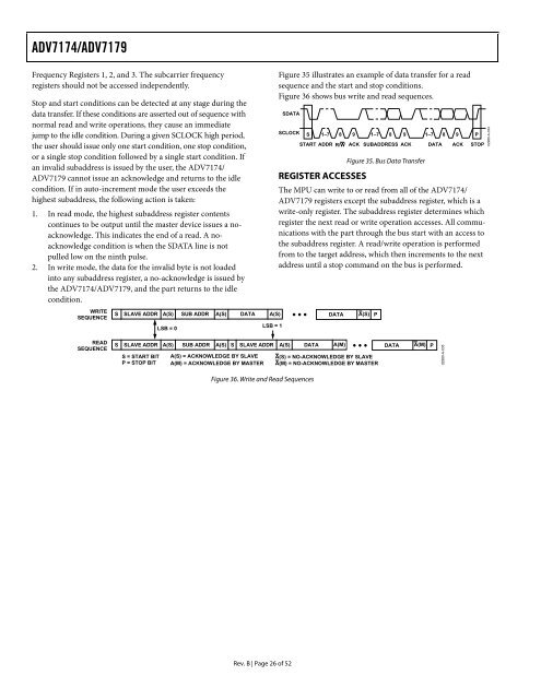
Figure 35 illustrates an example of data transfer for a read<br />
sequence and the start and stop conditions.<br />
Figure 36 shows bus write and read sequences.<br />
SDATA<br />
SCLOCK<br />
S<br />
1–7 8 9 1–7 8 9 1–7 8 9 P<br />
START ADDR R/W ACK SUBADDRESS ACK DATA ACK STOP<br />
Figure 35. Bus Data Transfer<br />
REGISTER ACCESSES<br />
The MPU can write to or read from all of the <strong>ADV7174</strong>/<br />
<strong>ADV7179</strong> registers except the subaddress register, which is a<br />
write-only register. The subaddress register determines which<br />
register the next read or write operation accesses. All communications<br />
with the part through the bus start with an access to<br />
the subaddress register. A read/write operation is performed<br />
from to the target address, which then increments to the next<br />
address until a stop command on the bus is performed.<br />
DATA A(S) P<br />
S SLAVE ADDR A(S) SUB ADDR A(S) S SLAVE ADDR A(S) DATA A(M) DATA A(M) P<br />
S = START BIT<br />
P = STOP BIT<br />
A(S) = ACKNOWLEDGE BY SLAVE<br />
A(M) = ACKNOWLEDGE BY MASTER<br />
Figure 36. Write and Read Sequences<br />
A(S) = NO-ACKNOWLEDGE BY SLAVE<br />
A(M) = NO-ACKNOWLEDGE BY MASTER<br />
02980-A-035<br />
02980-A-034


