

ADV7174/ADV7179 Chip Scale PAL/NTSC Video ... - Analog Devices
ADV7174/ADV7179 Chip Scale PAL/NTSC Video ... - Analog Devices
ADV7174/ADV7179 Chip Scale PAL/NTSC Video ... - Analog Devices

You also want an ePaper? Increase the reach of your titles
YUMPU automatically turns print PDFs into web optimized ePapers that Google loves.
<strong>ADV7174</strong>/<strong>ADV7179</strong><br />
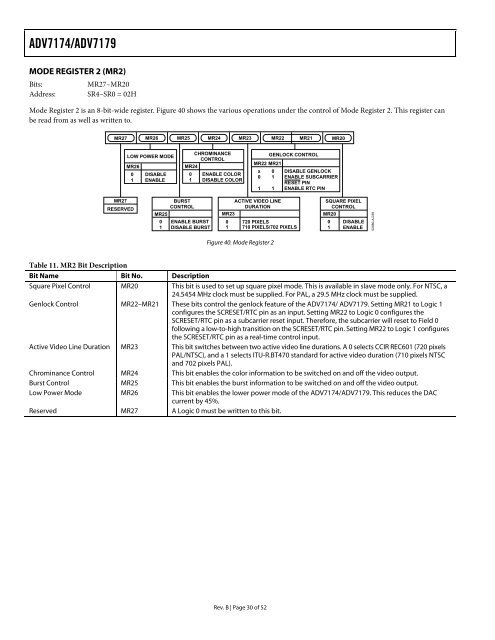
MODE REGISTER 2 (MR2)<br />
Bits: MR27–MR20<br />
Address: SR4–SR0 = 02H<br />
Mode Register 2 is an 8-bit-wide register. Figure 40 shows the various operations under the control of Mode Register 2. This register can<br />
be read from as well as written to.<br />
MR27 MR26 MR25 MR24 MR23 MR22 MR21 MR20<br />
LOW POWER MODE<br />
MR26<br />
0 DISABLE<br />
1 ENABLE<br />
CHROMINANCE<br />
CONTROL<br />
MR24<br />
0 ENABLE COLOR<br />
1 DISABLE COLOR<br />
Rev. B | Page 30 of 52<br />
GENLOCK CONTROL<br />
MR22 MR21<br />
x 0 DISABLE GENLOCK<br />
0 1 ENABLE SUBCARRIER<br />
RESET PIN<br />
1 1 ENABLE RTC PIN<br />
MR27 BURST<br />
ACTIVE VIDEO LINE<br />
RESERVED<br />
CONTROL<br />
DURATION<br />
MR25<br />
MR23<br />
0 ENABLE BURST 0 720 PIXELS<br />
1 DISABLE BURST 1 710 PIXELS/702 PIXELS<br />
Figure 40. Mode Register 2<br />
SQUARE PIXEL<br />
CONTROL<br />
MR20<br />
0 DISABLE<br />
1 ENABLE<br />
Table 11. MR2 Bit Description<br />
Bit Name Bit No. Description<br />
Square Pixel Control MR20 This bit is used to set up square pixel mode. This is available in slave mode only. For <strong>NTSC</strong>, a<br />
24.5454 MHz clock must be supplied. For <strong>PAL</strong>, a 29.5 MHz clock must be supplied.<br />
Genlock Control MR22–MR21 These bits control the genlock feature of the <strong>ADV7174</strong>/ <strong>ADV7179</strong>. Setting MR21 to Logic 1<br />
configures the SCRESET/RTC pin as an input. Setting MR22 to Logic 0 configures the<br />
SCRESET/RTC pin as a subcarrier reset input. Therefore, the subcarrier will reset to Field 0<br />
following a low-to-high transition on the SCRESET/RTC pin. Setting MR22 to Logic 1 configures<br />
the SCRESET/RTC pin as a real-time control input.<br />
Active <strong>Video</strong> Line Duration MR23 This bit switches between two active video line durations. A 0 selects CCIR REC601 (720 pixels<br />
<strong>PAL</strong>/<strong>NTSC</strong>), and a 1 selects ITU-R.BT470 standard for active video duration (710 pixels <strong>NTSC</strong><br />
and 702 pixels <strong>PAL</strong>).<br />
Chrominance Control MR24 This bit enables the color information to be switched on and off the video output.<br />
Burst Control MR25 This bit enables the burst information to be switched on and off the video output.<br />
Low Power Mode MR26 This bit enables the lower power mode of the <strong>ADV7174</strong>/<strong>ADV7179</strong>. This reduces the DAC<br />
current by 45%.<br />
Reserved MR27 A Logic 0 must be written to this bit.<br />
02980-A-039


