ADV7174/ADV7179 Chip Scale PAL/NTSC Video ... - Analog Devices
ADV7174/ADV7179 Chip Scale PAL/NTSC Video ... - Analog Devices
ADV7174/ADV7179 Chip Scale PAL/NTSC Video ... - Analog Devices
Create successful ePaper yourself
Turn your PDF publications into a flip-book with our unique Google optimized e-Paper software.
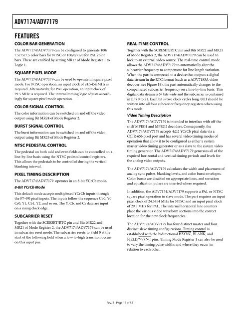
<strong>ADV7174</strong>/<strong>ADV7179</strong><br />
FEATURES<br />
COLOR BAR GENERATION<br />
The <strong>ADV7174</strong>/<strong>ADV7179</strong> can be configured to generate 100/<br />
7.5/75/7.5 color bars for <strong>NTSC</strong> or 100/0/75/0 for <strong>PAL</strong> color<br />
bars. These are enabled by setting MR17 of Mode Register 1 to<br />
Logic 1.<br />
SQUARE PIXEL MODE<br />
The <strong>ADV7174</strong>/<strong>ADV7179</strong> can be used to operate in square pixel<br />
mode. For <strong>NTSC</strong> operation, an input clock of 24.5454 MHz is<br />
required. Alternatively, for <strong>PAL</strong> operation, an input clock of<br />
29.5 MHz is required. The internal timing logic adjusts accordingly<br />
for square pixel mode operation.<br />
COLOR SIGNAL CONTROL<br />
The color information can be switched on and off the video<br />
output using Bit MR24 of Mode Register 2.<br />
BURST SIGNAL CONTROL<br />
The burst information can be switched on and off the video<br />
output using Bit MR25 of Mode Register 2.<br />
<strong>NTSC</strong> PEDESTAL CONTROL<br />
The pedestal on both odd and even fields can be controlled on a<br />
line-by-line basis using the <strong>NTSC</strong> pedestal control registers.<br />
This allows the pedestals to be controlled during the vertical<br />
blanking interval.<br />
PIXEL TIMING DESCRIPTION<br />
The <strong>ADV7174</strong>/<strong>ADV7179</strong> operates in an 8-bit YCrCb mode.<br />
8-Bit YCrCb Mode<br />
This default mode accepts multiplexed YCrCb inputs through<br />
the P7–P0 pixel inputs. The inputs follow the sequence Cb0, Y0<br />
Cr0, Y1, Cb1, Y2, and so on. The Y, Cb, and Cr data are input<br />
on a rising clock edge.<br />
SUBCARRIER RESET<br />
Together with the SCRESET/RTC pin and Bits MR22 and<br />
MR21 of Mode Register 2, the <strong>ADV7174</strong>/<strong>ADV7179</strong> can be used<br />
in subcarrier reset mode. The subcarrier resets to Field 0 at the<br />
start of the following field when a low-to-high transition occurs<br />
on this input pin.<br />
Rev. B | Page 16 of 52<br />
REAL-TIME CONTROL<br />
Together with the SCRESET/RTC pin and Bits MR22 and MR21<br />
of Mode Register 2, the <strong>ADV7174</strong>/<strong>ADV7179</strong> can be used to<br />
lock to an external video source. The real-time control mode<br />
allows the <strong>ADV7174</strong>/<strong>ADV7179</strong> to automatically alter the<br />
subcarrier frequency to compensate for line length variation.<br />
When the part is connected to a device that outputs a digital<br />
data stream in the RTC format (such as a ADV7183A video<br />
decoder; see Figure 19), the part automatically changes to the<br />
compensated subcarrier frequency on a line-by-line basis. This<br />
digital data stream is 67 bits wide and the subcarrier is contained<br />
in Bits 0 to 21. Each bit is two clock cycles long. 00H should be<br />
written into all four subcarrier frequency registers when using<br />
this mode.<br />
<strong>Video</strong> Timing Description<br />
The <strong>ADV7174</strong>/<strong>ADV7179</strong> is intended to interface with off-theshelf<br />
MPEG1 and MPEG2 decoders. Consequently, the<br />
<strong>ADV7174</strong>/<strong>ADV7179</strong> accepts 4:2:2 YCrCb pixel data via a<br />
CCIR-656 pixel port and has several video timing modes of<br />
operation that allow it to be configured as either a system<br />
master video timing generator or as a slave to the system video<br />
timing generator. The <strong>ADV7174</strong>/<strong>ADV7179</strong> generates all of the<br />
required horizontal and vertical timing periods and levels for<br />
the analog video outputs.<br />
The <strong>ADV7174</strong>/<strong>ADV7179</strong> calculates the width and placement of<br />
analog sync pulses, blanking levels, and color burst envelopes.<br />
Color bursts are disabled on appropriate lines, and serration<br />
and equalization pulses are inserted where required.<br />
In addition, the <strong>ADV7174</strong>/<strong>ADV7179</strong> supports a <strong>PAL</strong> or <strong>NTSC</strong><br />
square pixel operation in slave mode. The part requires an input<br />
pixel clock of 24.5454 MHz for <strong>NTSC</strong> and an input pixel clock<br />
of 29.5 MHz for <strong>PAL</strong>. The internal horizontal line counters<br />
place the various video waveform sections into the correct<br />
location for the new clock frequencies.<br />
The <strong>ADV7174</strong>/<strong>ADV7179</strong> has four distinct master and four<br />
distinct slave timing configurations. Timing control is<br />
established with the bidirectional HSYNC, BLANK, and<br />
FIELD/VSYNC pins. Timing Mode Register 1 can also be used<br />
to vary the timing pulse widths and where they occur in<br />
relation to each other.


