

ADV7174/ADV7179 Chip Scale PAL/NTSC Video ... - Analog Devices
ADV7174/ADV7179 Chip Scale PAL/NTSC Video ... - Analog Devices
ADV7174/ADV7179 Chip Scale PAL/NTSC Video ... - Analog Devices

Create successful ePaper yourself
Turn your PDF publications into a flip-book with our unique Google optimized e-Paper software.
<strong>ADV7174</strong>/<strong>ADV7179</strong><br />
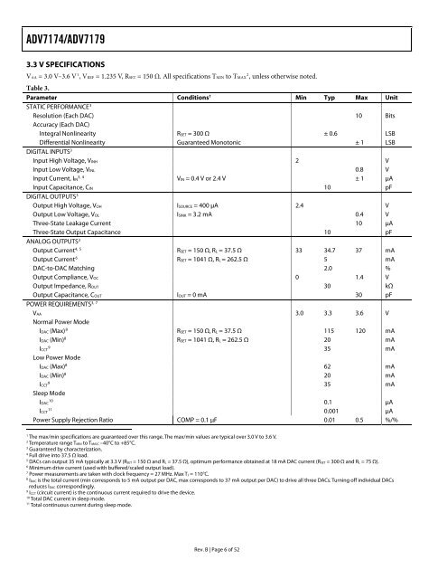
3.3 V SPECIFICATIONS<br />
VAA = 3.0 V–3.6 V 1 , VREF = 1.235 V, RSET = 150 Ω. All specifications TMIN to TMAX 2 , unless otherwise noted.<br />
Table 3.<br />
Parameter Conditions1 STATIC PERFORMANCE<br />
Min Typ Max Unit<br />
3<br />
Resolution (Each DAC)<br />
Accuracy (Each DAC)<br />
10 Bits<br />
Integral Nonlinearity RSET = 300 Ω ± 0.6 LSB<br />
Differential Nonlinearity<br />
DIGITAL INPUTS<br />
Guaranteed Monotonic ± 1 LSB<br />
3<br />
Input High Voltage, VINH 2 V<br />
Input Low Voltage, VINL 0.8 V<br />
Input Current, IIN 3, 4 VIN = 0.4 V or 2.4 V ± 1 μA<br />
Input Capacitance, CIN<br />
DIGITAL OUTPUTS<br />
10 pF<br />
3<br />
Output High Voltage, VOH ISOURCE = 400 μA 2.4 V<br />
Output Low Voltage, VOL ISINK = 3.2 mA 0.4 V<br />
Three-State Leakage Current 10 μA<br />
Three-State Output Capacitance<br />
ANALOG OUTPUTS<br />
10 pF<br />
3<br />
Output Current4, 5 RSET = 150 Ω, RL = 37.5 Ω 33 34.7 37 mA<br />
Output Current6 RSET = 1041 Ω, RL = 262.5 Ω 5 mA<br />
DAC-to-DAC Matching 2.0 %<br />
Output Compliance, VOC 0 1.4 V<br />
Output Impedance, ROUT 30 kΩ<br />
Output Capacitance, COUT<br />
3, 7<br />
POWER REQUIREMENTS<br />
IOUT = 0 mA 30 pF<br />
VAA<br />
Normal Power Mode<br />
3.0 3.3 3.6 V<br />
IDAC (Max) 8 RSET = 150 Ω, RL = 37.5 Ω 115 120 mA<br />
IDAC (Min) 8 RSET = 1041 Ω, RL = 262.5 Ω 20 mA<br />
ICCT 9 Low Power Mode<br />
35 mA<br />
IDAC (Max) 8 62 mA<br />
IDAC (Min) 8 20 mA<br />
ICCT 9 Sleep Mode<br />
35 mA<br />
IDAC 10 0.1 μA<br />
ICCT 11 0.001 μA<br />
Power Supply Rejection Ratio COMP = 0.1 μF 0.01 0.5 %/%<br />
1 The max/min specifications are guaranteed over this range. The max/min values are typical over 3.0 V to 3.6 V.<br />
2 Temperature range TMIN to TMAX: –40°C to +85°C.<br />
3 Guaranteed by characterization.<br />
4 Full drive into 37.5 Ω load.<br />
5 DACs can output 35 mA typically at 3.3 V (RSET = 150 Ω and RL = 37.5 Ω), optimum performance obtained at 18 mA DAC current (RSET = 300 Ω and RL = 75 Ω).<br />
6 Minimum drive current (used with buffered/scaled output load).<br />
7 Power measurements are taken with clock frequency = 27 MHz. Max TJ = 110°C.<br />
8 IDAC is the total current (min corresponds to 5 mA output per DAC, max corresponds to 37 mA output per DAC) to drive all three DACs. Turning off individual DACs<br />
reduces IDAC correspondingly.<br />
9 ICCT (circuit current) is the continuous current required to drive the device.<br />
10 Total DAC current in sleep mode.<br />
11 Total continuous current during sleep mode.<br />
Rev. B | Page 6 of 52


