

ADV7174/ADV7179 Chip Scale PAL/NTSC Video ... - Analog Devices
ADV7174/ADV7179 Chip Scale PAL/NTSC Video ... - Analog Devices
ADV7174/ADV7179 Chip Scale PAL/NTSC Video ... - Analog Devices

You also want an ePaper? Increase the reach of your titles
YUMPU automatically turns print PDFs into web optimized ePapers that Google loves.
<strong>ADV7174</strong>/<strong>ADV7179</strong><br />
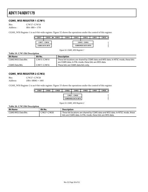
CGMS_WSS REGISTER 1 (C/W1)<br />
Bits: C/W17–C/W10<br />
Address : SR4–SR0 = 17H<br />
CGMS_WSS Register 1 is an 8-bit-wide register. Figure 52 shows the operations under the control of this register.<br />
C/W17 C/W16 C/W15 C/W14 C/W13 C/W12 C/W11 C/W10<br />
C/W17 – C/W16<br />
CGMS DATA BITS<br />
Rev. B | Page 38 of 52<br />
C/W15 – C/W10<br />
CGMS/WSS DATA BITS<br />
Figure 52. CGMS_WSS Register 1<br />
Table 19. C/W1 Bit Description<br />
Bit Name Bit No. Description<br />
CGMS/WSS Data Bits C/W15–C/W10 These bit locations are shared by CGMS data and WSS data. In <strong>NTSC</strong> mode, these bits<br />
are CGMS data. In <strong>PAL</strong> mode, these bits are WSS data.<br />
CGMS Data Bits C/W17–C/W16 These bits are CGMS data bits only.<br />
CGMS_WSS REGISTER 2 (C/W2)<br />
Bits: C/W27–C/W20<br />
Address: (SR4–SR00) = 18H<br />
CGMS_WSS Register 2 is an 8-bit-wide register. Figure 53 shows the operations under the control of this register.<br />
C/W27 C/W26 C/W25 C/W24 C/W23 C/W22 C/W21 C/W20<br />
C/W27 – C/W20<br />
CGMS/WSS DATA BITS<br />
Figure 53. CGMS_WSS Register 2<br />
Table 20. C/W2 Bit Description<br />
Bit Name Bit No. Description<br />
CGMS/WSS Data Bits C/W27–C/W20 These bit locations are shared by CGMS data and WSS data. In <strong>NTSC</strong> mode, these<br />
bits are CGMS data. In <strong>PAL</strong> mode, these bits are WSS data.<br />
02980-A-051<br />
02980-A-052


