

ADV7174/ADV7179 Chip Scale PAL/NTSC Video ... - Analog Devices
ADV7174/ADV7179 Chip Scale PAL/NTSC Video ... - Analog Devices
ADV7174/ADV7179 Chip Scale PAL/NTSC Video ... - Analog Devices

You also want an ePaper? Increase the reach of your titles
YUMPU automatically turns print PDFs into web optimized ePapers that Google loves.
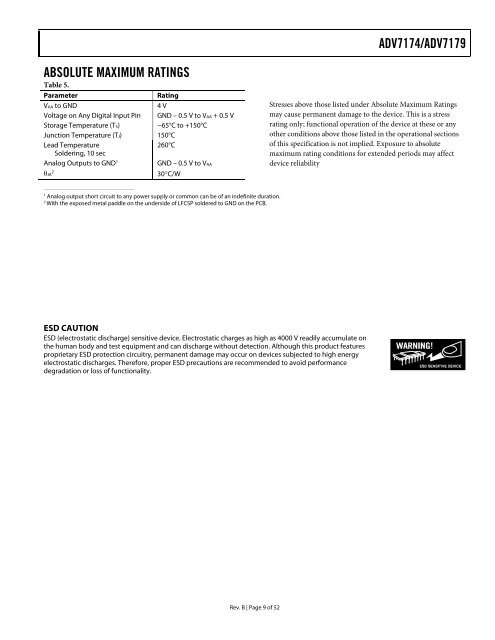
ABSOLUTE MAXIMUM RATINGS<br />
Table 5.<br />
Parameter Rating<br />
VAA to GND 4 V<br />
Voltage on Any Digital Input Pin GND – 0.5 V to VAA + 0.5 V<br />
Storage Temperature (TS) −65°C to +150°C<br />
Junction Temperature (TJ) 150°C<br />
Lead Temperature<br />
Soldering, 10 sec<br />
260°C<br />
<strong>Analog</strong> Outputs to GND1 GND – 0.5 V to VAA<br />
θJA 2 30°C/W<br />
__________________________________________________<br />
1 <strong>Analog</strong> output short circuit to any power supply or common can be of an indefinite duration.<br />
2 With the exposed metal paddle on the underside of LFCSP soldered to GND on the PCB.<br />
Rev. B | Page 9 of 52<br />
<strong>ADV7174</strong>/<strong>ADV7179</strong><br />
Stresses above those listed under Absolute Maximum Ratings<br />
may cause permanent damage to the device. This is a stress<br />
rating only; functional operation of the device at these or any<br />
other conditions above those listed in the operational sections<br />
of this specification is not implied. Exposure to absolute<br />
maximum rating conditions for extended periods may affect<br />
device reliability<br />
ESD CAUTION<br />
ESD (electrostatic discharge) sensitive device. Electrostatic charges as high as 4000 V readily accumulate on<br />
the human body and test equipment and can discharge without detection. Although this product features<br />
proprietary ESD protection circuitry, permanent damage may occur on devices subjected to high energy<br />
electrostatic discharges. Therefore, proper ESD precautions are recommended to avoid performance<br />
degradation or loss of functionality.


