

ADV7174/ADV7179 Chip Scale PAL/NTSC Video ... - Analog Devices
ADV7174/ADV7179 Chip Scale PAL/NTSC Video ... - Analog Devices
ADV7174/ADV7179 Chip Scale PAL/NTSC Video ... - Analog Devices

Create successful ePaper yourself
Turn your PDF publications into a flip-book with our unique Google optimized e-Paper software.
<strong>ADV7174</strong>/<strong>ADV7179</strong><br />
SUPPLY DECOUPLING<br />
For optimum performance, bypass capacitors should be installed<br />
using the shortest leads possible, consistent with reliable<br />
operation, to reduce the lead inductance. Best performance is<br />
obtained with 0.1 μF ceramic capacitor decoupling. Each group<br />
of VAA pins on the <strong>ADV7174</strong>/<strong>ADV7179</strong> must have at least one<br />
0.1 μF decoupling capacitor to GND. These capacitors should<br />
be placed as close to the device as possible.<br />
It is important to note that while the <strong>ADV7174</strong>/<strong>ADV7179</strong><br />
contains circuitry to reject power supply noise, this rejection<br />
decreases with frequency. If a high frequency switching power<br />
supply is used, the designer should pay close attention to<br />
reducing power supply noise and consider using a 3-terminal<br />
voltage regulator for supplying power to the analog power<br />
plane.<br />
DIGITAL SIGNAL INTERCONNECT<br />
The digital inputs to the <strong>ADV7174</strong>/<strong>ADV7179</strong> should be<br />
isolated as much as possible from the analog outputs and other<br />
analog circuitry. Also, these input signals should not overlay the<br />
analog power plane.<br />
Due to the high clock rates involved, long clock lines to the<br />
<strong>ADV7174</strong>/<strong>ADV7179</strong> should be avoided to reduce noise pickup.<br />
Any active termination resistors for the digital inputs should be<br />
connected to the regular PCB power plane (VCC) and not to the<br />
analog power plane.<br />
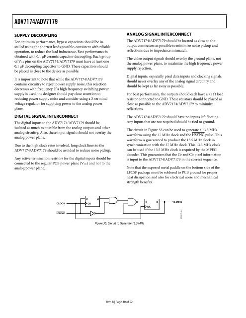
CLOCK<br />
HSYNC<br />
D Q<br />
CK<br />
Figure 55. Circuit to Generate 13.5 MHz<br />
Rev. B | Page 40 of 52<br />
ANALOG SIGNAL INTERCONNECT<br />
The <strong>ADV7174</strong>/<strong>ADV7179</strong> should be located as close to the<br />
output connectors as possible to minimize noise pickup and<br />
reflections due to impedance mismatch.<br />
The video output signals should overlay the ground plane, not<br />
the analog power plane, to maximize the high frequency power<br />
supply rejection.<br />
Digital inputs, especially pixel data inputs and clocking signals,<br />
should never overlay any of the analog signal circuitry and<br />
should be kept as far away as possible.<br />
For best performance, the outputs should each have a 75 Ω load<br />
resistor connected to GND. These resistors should be placed as<br />
close as possible to the <strong>ADV7174</strong>/<strong>ADV7179</strong> to minimize<br />
reflections.<br />
The <strong>ADV7174</strong>/<strong>ADV7179</strong> should have no inputs left floating.<br />
Any inputs that are not required should be tied to ground.<br />
The circuit in Figure 55 can be used to generate a 13.5 MHz<br />
waveform using the 27 MHz clock and the HSYNC pulse. This<br />
waveform is guaranteed to produce the 13.5 MHz clock in<br />
synchronization with the 27 MHz clock. This 13.5 MHz clock<br />
can be used if the 13.5 MHz clock is required by the MPEG<br />
decoder. This guarantees that the Cr and Cb pixel information<br />
is input to the <strong>ADV7174</strong>/<strong>ADV7179</strong> in the correct sequence.<br />
Note that the exposed metal paddle on the bottom side of the<br />
LFCSP package must be soldered to PCB ground for proper<br />
heat dissipation and also for electrical noise and mechanical<br />
strength benefits.<br />
D Q<br />
CK<br />
13.5MHz<br />
02980-A-054


