

ADV7174/ADV7179 Chip Scale PAL/NTSC Video ... - Analog Devices
ADV7174/ADV7179 Chip Scale PAL/NTSC Video ... - Analog Devices
ADV7174/ADV7179 Chip Scale PAL/NTSC Video ... - Analog Devices

Create successful ePaper yourself
Turn your PDF publications into a flip-book with our unique Google optimized e-Paper software.
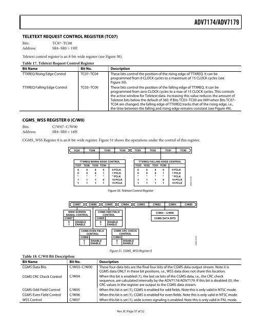
TELETEXT REQUEST CONTROL REGISTER (TC07)<br />
Bits: TC07–TC00<br />
Address: SR4–SR0 = 19H<br />
Rev. B | Page 37 of 52<br />
<strong>ADV7174</strong>/<strong>ADV7179</strong><br />
Teletext control register is an 8-bit-wide register (see Figure 50).<br />
Table 17. Teletext Request Control Register<br />
Bit Name Bit No. Description<br />
TTXREQ Rising Edge Control TC07–TC04 These bits control the position of the rising edge of TTXREQ. It can be<br />
programmed from 0 CLOCK cycles to a maximum of 15 CLOCK cycles (see<br />
Figure 50).<br />
TTXREQ Falling Edge Control TC03–TC00 These bits control the position of the falling edge of TTXREQ. It can be<br />
programmed from zero CLOCK cycles to a max of 15 CLOCK cycles. This controls<br />
the active window for Teletext data. Increasing this value reduces the amount of<br />
Teletext bits below the default of 360. If Bits TC03–TC00 are 00H when Bits TC07–<br />
TC04 are changed, the falling edge of TTXREQ tracks that of the rising edge, i.e.,<br />
the time between the falling and rising edge remains constant (see Figure 49).<br />
CGMS_WSS REGISTER 0 (C/W0)<br />
Bits: C/W07–C/W00<br />
Address: SR4–SR0 = 16H<br />
CGMS_WSS Register 0 is an 8-bit-wide register. Figure 51 shows the operations under the control of this register.<br />
TC07 TC06 TC05 TC04 TC03 TC02<br />
TTXREQ RISING EDGE CONTROL<br />
TC07 TC06 TC05 TC04<br />
0 0 0 0 0 PCLK<br />
0 0 0 1 1PCLK<br />
" " " " "PCLK<br />
1 1 1 0 14 PCLK<br />
1 1 1 1 15 PCLK<br />
Figure 50. Teletext Control Register<br />
TC01 TC00<br />
TTXREQ FALLING EDGE CONTROL<br />
TC03 TC02 TC01 TC00<br />
0 0 0 0 0PCLK<br />
0 0 0 1 1PCLK<br />
" " " " "PCLK<br />
1 1 1 0 14 PCLK<br />
1 1 1 1 15 PCLK<br />
C/W07 C/W06 C/W05 C/W04 C/W03 C/W02 C/W01 C/W00<br />
WIDE SCREEN<br />
SIGNAL CONTROL<br />
C/W07<br />
0 DISABLE<br />
1 ENABLE<br />
CGMS EVEN FIELD<br />
CONTROL<br />
C/W06<br />
0 DISABLE<br />
1 ENABLE<br />
CGMS ODD FIELD<br />
CONTROL<br />
C/W05<br />
0 DISABLE<br />
1 ENABLE<br />
CGMS CRC CHECK<br />
CONTROL<br />
C/W04<br />
0 DISABLE<br />
1 ENABLE<br />
C/W03 – C/W00<br />
CGMS DATA BITS<br />
Figure 51. CGMS_WSS Register 0<br />
Table 18. C/W0 Bit Description<br />
Bit Name Bit No. Description<br />
CGMS Data Bits C/W03–C/W00 These four data bits are the final four bits of the CGMS data output stream. Note it is<br />
CGMS data ONLY in these bit positions, i.e., WSS data does not share this location.<br />
CGMS CRC Check Control C/W04 When this bit is enabled (1), the last six bits of the CGMS data, i.e., the CRC check<br />
sequence, are calculated internally by the <strong>ADV7174</strong>/<strong>ADV7179</strong>. If this bit is disabled (0), the<br />
CRC values in the register are output to the CGMS data stream.<br />
CGMS Odd Field Control C/W05 When this bit is set (1), CGMS is enabled for odd fields. Note this is only valid in <strong>NTSC</strong> mode.<br />
CGMS Even Field Control C/W06 When this bit is set (1), CGMS is enabled for even fields. Note this is only valid in <strong>NTSC</strong> mode.<br />
WSS Control C/W07 When this bit is set (1), wide screen signaling is enabled. Note this is only valid in <strong>PAL</strong> mode.<br />
02980-A-049<br />
02980-A-050


