

ADV7174/ADV7179 Chip Scale PAL/NTSC Video ... - Analog Devices
ADV7174/ADV7179 Chip Scale PAL/NTSC Video ... - Analog Devices
ADV7174/ADV7179 Chip Scale PAL/NTSC Video ... - Analog Devices

You also want an ePaper? Increase the reach of your titles
YUMPU automatically turns print PDFs into web optimized ePapers that Google loves.
<strong>ADV7174</strong>/<strong>ADV7179</strong><br />
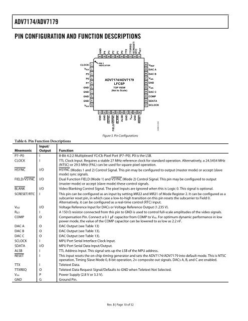
PIN CONFIGURATION AND FUNCTION DESCRIPTIONS<br />
CLOCK 1<br />
VAA 2<br />
P5 3<br />
P6 4<br />
P7 5<br />
GND 6<br />
GND 7<br />
GND 8<br />
GND 9<br />
VAA 10<br />
GND<br />
P4<br />
P3<br />
P2<br />
P1<br />
P0<br />
TTX<br />
40 39 38 37 36 35 34 33 32 31<br />
PIN 1<br />
INDICATOR<br />
11 12 13 14 15 16 17 18 19 20<br />
GND<br />
GND<br />
HSYNC<br />
FIELD/VSYNC<br />
BLANK<br />
TTXREQ<br />
<strong>ADV7174</strong>/<strong>ADV7179</strong><br />
LFCSP<br />
TOP VIEW<br />
(Not to <strong>Scale</strong>)<br />
ALSB<br />
GND<br />
VAA GND<br />
RESET<br />
Rev. B | Page 10 of 52<br />
SCRESET/<br />
RTC<br />
R SET<br />
30 VREF<br />
29 DAC A<br />
28 DAC B<br />
27 VAA 26 GND<br />
25 VAA 24 DAC C<br />
23 COMP<br />
22 SDATA<br />
21 SCLOCK<br />
Figure 5. Pin Configurations<br />
Table 6. Pin Function Descriptions<br />
Input/<br />
Mnemonic Output Function<br />
P7–P0 I 8-Bit 4:2:2 Multiplexed YCrCb Pixel Port (P7–P0). P0 is the LSB.<br />
CLOCK I TTL Clock Input. Requires a stable 27 MHz reference clock for standard operation. Alternatively, a 24.5454 MHz<br />
(<strong>NTSC</strong>) or 29.5 MHz (<strong>PAL</strong>) can be used for square pixel operation.<br />
HSYNC I/O HSYNC (Modes 1 and 2) Control Signal. This pin may be configured to output (master mode) or accept (slave<br />
mode) sync signals.<br />
FIELD/VSYNC I/O Dual Function FIELD (Mode 1) and VSYNC (Mode 2) Control Signal. This pin may be configured to output<br />
(master mode) or accept (slave mode) these control signals.<br />
BLANK I/O <strong>Video</strong> Blanking Control Signal. The pixel inputs are ignored when this is Logic 0. This signal is optional.<br />
SCRESET/RTC I This pin can be configured as an input by setting MR22 and MR21 of Mode Register 2. It can be configured as a<br />
subcarrier reset pin, in which case a low-to-high transition on this pin resets the subcarrier to Field 0.<br />
Alternatively, it can be configured as a real-time control (RTC) input.<br />
VREF I/O Voltage Reference Input for DACs or Voltage Reference Output (1.235 V).<br />
RSET I A 150 Ω resistor connected from this pin to GND is used to control full-scale amplitudes of the video signals.<br />
COMP O Compensation Pin. Connect a 0.1 μF capacitor from COMP to VAA. For optimum dynamic performance in low<br />
power mode, the value of the COMP capacitor can be lowered to as low as 2.2 nF.<br />
DAC A O DAC Output (see Table 13)<br />
DAC B O DAC Output (see Table 13).<br />
DAC C O DAC Output (see Table 13).<br />
SCLOCK I MPU Port Serial Interface Clock Input.<br />
SDATA I/O MPU Port Serial Data Input/Output.<br />
ALSB I TTL Address Input. This signal sets up the LSB of the MPU address.<br />
RESET I This input resets the on-chip timing generator and sets the <strong>ADV7174</strong>/<strong>ADV7179</strong> into default mode. This is <strong>NTSC</strong><br />
operation, Timing Slave Mode 0, 8-bit operation, 2× composite out signals. DACs A, B, and C are enabled.<br />
TTX I Teletext Data.<br />
TTXREQ O Teletext Data Request Signal/Defaults to GND when Teletext Not Selected.<br />
VAA P Power Supply (2.8 V or 3.3 V).<br />
GND G Ground Pin.<br />
02980-A-005


