

ADV7174/ADV7179 Chip Scale PAL/NTSC Video ... - Analog Devices
ADV7174/ADV7179 Chip Scale PAL/NTSC Video ... - Analog Devices
ADV7174/ADV7179 Chip Scale PAL/NTSC Video ... - Analog Devices

Create successful ePaper yourself
Turn your PDF publications into a flip-book with our unique Google optimized e-Paper software.
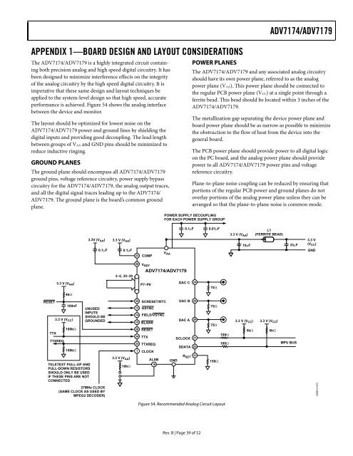
APPENDIX 1—BOARD DESIGN AND LAYOUT CONSIDERATIONS<br />
The <strong>ADV7174</strong>/<strong>ADV7179</strong> is a highly integrated circuit containing<br />
both precision analog and high speed digital circuitry. It has<br />
been designed to minimize interference effects on the integrity<br />
of the analog circuitry by the high speed digital circuitry. It is<br />
imperative that these same design and layout techniques be<br />
applied to the system-level design so that high speed, accurate<br />
performance is achieved. Figure 54 shows the analog interface<br />
between the device and monitor.<br />
The layout should be optimized for lowest noise on the<br />
<strong>ADV7174</strong>/<strong>ADV7179</strong> power and ground lines by shielding the<br />
digital inputs and providing good decoupling. The lead length<br />
between groups of VAA and GND pins should be minimized to<br />
Rev. B | Page 39 of 52<br />
<strong>ADV7174</strong>/<strong>ADV7179</strong><br />
POWER PLANES<br />
The <strong>ADV7174</strong>/<strong>ADV7179</strong> and any associated analog circuitry<br />
should have its own power plane, referred to as the analog<br />
power plane (VAA). This power plane should be connected to<br />
the regular PCB power plane (VCC) at a single point through a<br />
ferrite bead. This bead should be located within 3 inches of the<br />
<strong>ADV7174</strong>/<strong>ADV7179</strong>.<br />
The metallization gap separating the device power plane and<br />
board power plane should be as narrow as possible to minimize<br />
the obstruction to the flow of heat from the device into the<br />
general board.<br />
reduce inductive ringing. The PCB power plane should provide power to all digital logic<br />
GROUND PLANES<br />
The ground plane should encompass all <strong>ADV7174</strong>/<strong>ADV7179</strong><br />
ground pins, voltage reference circuitry, power supply bypass<br />
circuitry for the <strong>ADV7174</strong>/<strong>ADV7179</strong>, the analog output traces,<br />
and all the digital signal traces leading up to the <strong>ADV7174</strong>/<br />
<strong>ADV7179</strong>. The ground plane is the board’s common ground<br />
plane.<br />
RESET<br />
TTX<br />
3.3 V (V AA )<br />
3.3 V (V CC )<br />
TTXREQ<br />
4kΩ<br />
100nF<br />
100kΩ<br />
100kΩ<br />
TELETEXT PULL-UP AND<br />
PULL-DOWN RESISTORS<br />
SHOULD ONLY BE USED<br />
IF THESE PINS ARE NOT<br />
CONNECTED<br />
3.3V (V AA )<br />
0.1μF<br />
UNUSED<br />
INPUTS<br />
SHOULD BE<br />
GROUNDED<br />
27MHz CLOCK<br />
(SAME CLOCK AS USED BY<br />
MPEG2 DECODER)<br />
3.3 V (V AA )<br />
0.1μF<br />
3–5, 35–39<br />
3.3 V (V AA )<br />
10kΩ<br />
23<br />
30<br />
32<br />
13<br />
14<br />
15<br />
20<br />
COMP<br />
V REF<br />
P7–P0<br />
SCRESET/RTC<br />
HSYNC<br />
FIELD/VSYNC<br />
BLANK<br />
RESET<br />
CLOCK<br />
ALSB<br />
16<br />
on the PC board, and the analog power plane should provide<br />
power to all <strong>ADV7174</strong>/<strong>ADV7179</strong> power pins and voltage<br />
reference circuitry.<br />
Plane-to-plane noise coupling can be reduced by ensuring that<br />
portions of the regular PCB power and ground planes do not<br />
overlay portions of the analog power plane unless they can be<br />
arranged so that the plane-to-plane noise is common mode.<br />
POWER SUPPLY DECOUPLING<br />
FOR EACH POWER SUPPLY GROUP<br />
V AA<br />
<strong>ADV7174</strong>/<strong>ADV7179</strong><br />
34 TTX<br />
33 TTXREQ<br />
1<br />
GND<br />
DAC C<br />
DAC B<br />
DAC A<br />
SCLOCK<br />
0.1μF 0.01μF<br />
24<br />
28<br />
29<br />
21<br />
SDATA 22<br />
R 31<br />
SET<br />
75Ω<br />
75Ω<br />
75Ω<br />
150Ω<br />
100Ω<br />
100Ω<br />
Figure 54. Recommended <strong>Analog</strong> Circuit Layout<br />
3.3 V (V AA )<br />
10μF<br />
3.3 V (V CC )<br />
5kΩ<br />
L1<br />
(FERRITE BEAD)<br />
3.3 V (V CC )<br />
5kΩ<br />
33μF<br />
MPU BUS<br />
3.3 V<br />
(VCC )<br />
GND<br />
02980-A-053


