

ADV7174/ADV7179 Chip Scale PAL/NTSC Video ... - Analog Devices
ADV7174/ADV7179 Chip Scale PAL/NTSC Video ... - Analog Devices
ADV7174/ADV7179 Chip Scale PAL/NTSC Video ... - Analog Devices

You also want an ePaper? Increase the reach of your titles
YUMPU automatically turns print PDFs into web optimized ePapers that Google loves.
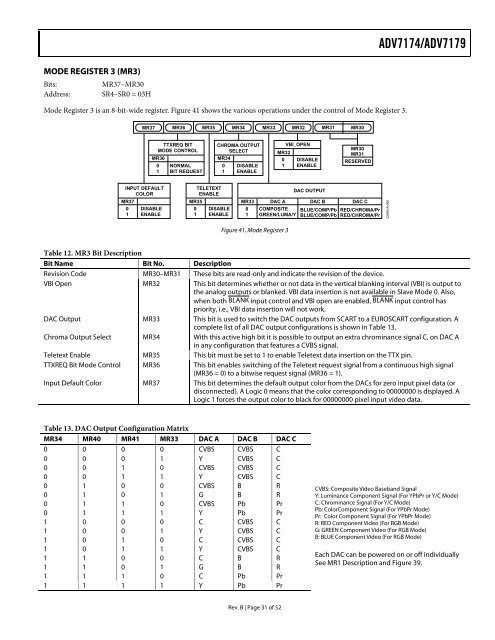
MODE REGISTER 3 (MR3)<br />
Bits: MR37–MR30<br />
Address: SR4–SR0 = 03H<br />
Mode Register 3 is an 8-bit-wide register. Figure 41 shows the various operations under the control of Mode Register 3.<br />
MR37 MR36 MR35 MR34 MR33 MR32<br />
INPUT DEFAULT<br />
COLOR<br />
MR37<br />
0 DISABLE<br />
1 ENABLE<br />
TTXREQ BIT<br />
MODE CONTROL<br />
MR36<br />
0 NORMAL<br />
1 BIT REQUEST<br />
TELETEXT<br />
ENABLE<br />
MR35<br />
0 DISABLE<br />
1 ENABLE<br />
CHROMA OUTPUT<br />
SELECT<br />
MR34<br />
0 DISABLE<br />
1 ENABLE<br />
MR33 DAC A<br />
Rev. B | Page 31 of 52<br />
VBI_OPEN<br />
MR32<br />
0 DISABLE<br />
1 ENABLE<br />
0 COMPOSITE<br />
1 GREEN/LUMA/Y<br />
Figure 41. Mode Register 3<br />
DAC OUTPUT<br />
DAC B<br />
BLUE/COMP/Pb<br />
BLUE/COMP/Pb<br />
MR31 MR30<br />
MR30<br />
MR31<br />
RESERVED<br />
DAC C<br />
RED/CHROMA/Pr<br />
RED/CHROMA/Pr<br />
<strong>ADV7174</strong>/<strong>ADV7179</strong><br />
Table 12. MR3 Bit Description<br />
Bit Name Bit No. Description<br />
Revision Code MR30–MR31 These bits are read-only and indicate the revision of the device.<br />
VBI Open MR32 This bit determines whether or not data in the vertical blanking interval (VBI) is output to<br />
the analog outputs or blanked. VBI data insertion is not available in Slave Mode 0. Also,<br />
when both BLANK input control and VBI open are enabled, BLANK input control has<br />
priority, i.e., VBI data insertion will not work.<br />
DAC Output MR33 This bit is used to switch the DAC outputs from SCART to a EUROSCART configuration. A<br />
complete list of all DAC output configurations is shown in Table 13.<br />
Chroma Output Select MR34 With this active high bit it is possible to output an extra chrominance signal C, on DAC A<br />
in any configuration that features a CVBS signal.<br />
Teletext Enable MR35 This bit must be set to 1 to enable Teletext data insertion on the TTX pin.<br />
TTXREQ Bit Mode Control MR36 This bit enables switching of the Teletext request signal from a continuous high signal<br />
(MR36 = 0) to a bitwise request signal (MR36 = 1).<br />
Input Default Color MR37 This bit determines the default output color from the DACs for zero input pixel data (or<br />
disconnected). A Logic 0 means that the color corresponding to 00000000 is displayed. A<br />
Logic 1 forces the output color to black for 00000000 pixel input video data.<br />
Table 13. DAC Output Configuration Matrix<br />
MR34 MR40 MR41 MR33 DAC A DAC B DAC C<br />
0 0 0 0 CVBS CVBS C<br />
0 0 0 1 Y CVBS C<br />
0 0 1 0 CVBS CVBS C<br />
0 0 1 1 Y CVBS C<br />
0 1 0 0 CVBS B R<br />
0 1 0 1 G B R<br />
0 1 1 0 CVBS Pb Pr<br />
0 1 1 1 Y Pb Pr<br />
1 0 0 0 C CVBS C<br />
1 0 0 1 Y CVBS C<br />
1 0 1 0 C CVBS C<br />
1 0 1 1 Y CVBS C<br />
1 1 0 0 C B R<br />
1 1 0 1 G B R<br />
1 1 1 0 C Pb Pr<br />
1 1 1 1 Y Pb Pr<br />
02980-A-040<br />
CVBS: Composite <strong>Video</strong> Baseband Signal<br />
Y: Luminance Component Signal (For YPbPr or Y/C Mode)<br />
C: Chrominance Signal (For Y/C Mode)<br />
Pb: ColorComponent Signal (For YPbPr Mode)<br />
Pr: Color Component Signal (For YPbPr Mode)<br />
R: RED Component <strong>Video</strong> (For RGB Mode)<br />
G: GREEN Component <strong>Video</strong> (For RGB Mode)<br />
B: BLUE Component <strong>Video</strong> (For RGB Mode)<br />
Each DAC can be powered on or off individually<br />
See MR1 Description and Figure 39.


