

ADV7174/ADV7179 Chip Scale PAL/NTSC Video ... - Analog Devices
ADV7174/ADV7179 Chip Scale PAL/NTSC Video ... - Analog Devices
ADV7174/ADV7179 Chip Scale PAL/NTSC Video ... - Analog Devices

Create successful ePaper yourself
Turn your PDF publications into a flip-book with our unique Google optimized e-Paper software.
<strong>ADV7174</strong>/<strong>ADV7179</strong><br />
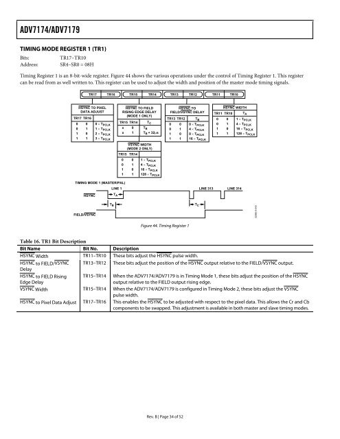
TIMING MODE REGISTER 1 (TR1)<br />
Bits: TR17–TR10<br />
Address: SR4–SR0 = 08H<br />
Timing Register 1 is an 8-bit-wide register. Figure 44 shows the various operations under the control of Timing Register 1. This register<br />
can be read from as well written to. This register can be used to adjust the width and position of the master mode timing signals.<br />
TR17 TR16 TR15 TR14 TR13 TR12<br />
HSYNC TO PIXEL<br />
DATA ADJUST<br />
TR17 TR16<br />
0 0 0 × TPCLK 0 1 1 × TPCLK 1 0 2 × TPCLK 1 1 3 × TPCLK HSYNC TO FIELD<br />
RISING EDGE DELAY<br />
(MODE 1 ONLY)<br />
TR15 TR14 TC x 0 TB x 1 TB + 32μs<br />
VSYNC WIDTH<br />
(MODE 2 ONLY)<br />
TR15 TR14<br />
0<br />
0<br />
1<br />
1<br />
TIMING MODE 1 (MASTER/<strong>PAL</strong>)<br />
LINE 1<br />
HSYNC<br />
TA FIELD/VSYNC<br />
T B<br />
0<br />
1<br />
0<br />
1<br />
1 × T PCLK<br />
4 × T PCLK<br />
16 × T PCLK<br />
128 × T PCLK<br />
Rev. B | Page 34 of 52<br />
HSYNC TO<br />
FIELD/VSYNC DELAY<br />
TR13 TR12<br />
0<br />
0<br />
1<br />
1<br />
0<br />
1<br />
0<br />
1<br />
Figure 44. Timing Register 1<br />
TB 0 × TPCLK 4 × TPCLK 8 × TPCLK 16 × TPCLK T C<br />
TR11 TR10<br />
HSYNC WIDTH<br />
TR11 TR10 TA 0 0 1 × TPCLK 0 1 4 × TPCLK 1 0 16 × TPCLK 1 1 128 × TPCLK LINE 313 LINE 314<br />
Table 16. TR1 Bit Description<br />
Bit Name Bit No. Description<br />
HSYNC Width<br />
TR11–TR10 These bits adjust the HSYNC pulse width.<br />
HSYNC to FIELD/VSYNC<br />
Delay<br />
TR13–TR12 These bits adjust the position of the HSYNC output relative to the FIELD/VSYNC output.<br />
HSYNC to FIELD Rising TR15–TR14 When the <strong>ADV7174</strong>/<strong>ADV7179</strong> is in Timing Mode 1, these bits adjust the position of the HSYNC<br />
Edge Delay<br />
output relative to the FIELD output rising edge.<br />
VSYNC Width<br />
TR15–TR14 When the <strong>ADV7174</strong>/<strong>ADV7179</strong> is configured in Timing Mode 2, these bits adjust the VSYNC<br />
pulse width.<br />
HSYNC to Pixel Data Adjust TR17–TR16<br />
This enables the HSYNC to be adjusted with respect to the pixel data. This allows the Cr and Cb<br />
components to be swapped. This adjustment is available in both master and slave timing modes.<br />
02980-A-043


