

ADV7174/ADV7179 Chip Scale PAL/NTSC Video ... - Analog Devices
ADV7174/ADV7179 Chip Scale PAL/NTSC Video ... - Analog Devices
ADV7174/ADV7179 Chip Scale PAL/NTSC Video ... - Analog Devices

Create successful ePaper yourself
Turn your PDF publications into a flip-book with our unique Google optimized e-Paper software.
RTC<br />
H/LTRANSITION<br />
COUNT START<br />
128<br />
COMPOSITE<br />
VIDEO<br />
(e.g., VCR<br />
OR CABLE)<br />
LOW<br />
13<br />
14 BITS<br />
RESERVED<br />
VIDEO<br />
DECODER<br />
(e.g., ADV7183A)<br />
0<br />
4 BITS<br />
RESERVED<br />
CLOCK<br />
SCRESET/RTC<br />
P7–P0<br />
HSYNC<br />
FIELD/VSYNC<br />
Rev. B | Page 17 of 52<br />
GREEN/LUMA/Y<br />
RED/CHROMA/Pr<br />
BLUE/COMPOSITE/Pb<br />
AD7174/<strong>ADV7179</strong><br />
5 BITS<br />
RESERVED<br />
<strong>ADV7174</strong>/<strong>ADV7179</strong><br />
SEQUENCE<br />
BIT2 TIME SLOT: 01 14 19<br />
67 68<br />
NOT USED IN THE<br />
<strong>ADV7174</strong>/<strong>ADV7179</strong><br />
21<br />
F SC PLL INCREMENT 1<br />
VALID<br />
SAMPLE<br />
INVALID<br />
SAMPLE<br />
NOTES<br />
1 FSC PLL INCREMENT IS 22 BITS LONG, VALUE LOADED INTO <strong>ADV7174</strong>/<strong>ADV7179</strong> F SC DDS REGISTER IS<br />
F SC PLL INCREMENT BITS 21:0 PLUS BITS 0:9 OF THE SUBCARRIER FREQUENCY REGISTERS. ALL ZEROS SHOULD<br />
BE WRITTEN TO THE SUBCARRIER FREQUENCY REGISTERS OF THE <strong>ADV7174</strong>/<strong>ADV7179</strong>.<br />
2 SEQUENCE BIT<br />
<strong>PAL</strong>: 0 = LINE NORMAL, 1 = LINE INVERTED<br />
<strong>NTSC</strong>: 0 = NO CHANGE<br />
3 RESET BIT<br />
RESET <strong>ADV7174</strong>/<strong>ADV7179</strong> DDS<br />
Vertical Blanking Data Insertion<br />
It is possible to allow encoding of incoming YCbCr data on<br />
those lines of VBI that do not bear line sync or pre-/postequalization<br />
pulses (see Figure 21 to Figure 32). This mode of<br />
operation is called partial blanking and is selected by setting<br />
MR32 to 1. It allows the insertion of any VBI data (opened VBI)<br />
into the encoded output waveform. This data is present in the<br />
digitized incoming YCbCr data stream, for example. WSS data,<br />
CGMS, VPS, and so on. Alternatively, the entire VBI may be<br />
blanked (no VBI data inserted) on these lines by setting MR32<br />
to 0.<br />
Mode 0 (CCIR-656): Slave Option<br />
(Timing Register 0 TR0 = X X X X X 0 0 0)<br />
The <strong>ADV7174</strong>/<strong>ADV7179</strong> is controlled by the SAV (start active<br />
video) and EAV (end active video) time codes in the pixel data.<br />
All timing information is transmitted using a 4-byte synchro-<br />
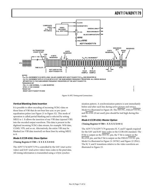
Figure 19. RTC Timing and Connections<br />
8/LLC<br />
0<br />
RESET<br />
BIT 3<br />
RESERVED<br />
nization pattern. A synchronization pattern is sent immediately<br />
before and after each line during active picture and retrace.<br />
Mode 0 is illustrated in Figure 20. The HSYNC, FIELD/VSYNC,<br />
and BLANK (if not used) pins should be tied high during this<br />
mode.<br />
Mode 0 (CCIR-656): Master Option<br />
(Timing Register 0 TR0 = X X X X X 0 0 1)<br />
The <strong>ADV7174</strong>/<strong>ADV7179</strong> generates H, V, and F signals required<br />
for the SAV and EAV time codes in the CCIR-656 standard. The<br />
H bit is output on the HSYNC pin, the V bit is output on the<br />
BLANK pin, and the F bit is output on the FIELD/VSYNC pin.<br />
Mode 0 is illustrated in Figure 21 (<strong>NTSC</strong>) and Figure 22 (<strong>PAL</strong>).<br />
The H, V, and F transitions relative to the video waveform are<br />
illustrated in Figure 23.<br />
02980-A-019


