

ADV7174/ADV7179 Chip Scale PAL/NTSC Video ... - Analog Devices
ADV7174/ADV7179 Chip Scale PAL/NTSC Video ... - Analog Devices
ADV7174/ADV7179 Chip Scale PAL/NTSC Video ... - Analog Devices

Create successful ePaper yourself
Turn your PDF publications into a flip-book with our unique Google optimized e-Paper software.
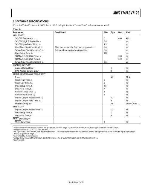
3.3 V TIMING SPECIFICATIONS<br />
VAA = 3.0 V–3.6 V 1 , VREF = 1.235 V, RSET = 150 Ω. All specifications TMIN to TMAX 2 , unless otherwise noted.<br />
Rev. B | Page 7 of 52<br />
<strong>ADV7174</strong>/<strong>ADV7179</strong><br />
Table 4.<br />
Parameter Conditions1 3, 4<br />
MPU PORT<br />
Min Typ Max Unit<br />
SCLOCK Frequency 0 400 kHz<br />
SCLOCK High Pulse Width, t1 0.6 μs<br />
SCLOCK Low Pulse Width, t2 1.3 μs<br />
Hold Time (Start Condition), t3 After this period, the first clock is generated 0.6 μs<br />
Setup Time (Start Condition), t4 Relevant for repeated start condition 0.6 μs<br />
Data Setup Time, t5 100 ns<br />
SDATA, SCLOCK Rise Time, t6 300 ns<br />
SDATA, SCLOCK Fall Time, t7 300 ns<br />
Setup Time (Stop Condition), t8<br />
3, 5<br />
ANALOG OUTPUTS<br />
0.6 μs<br />
<strong>Analog</strong> Output Delay 7 ns<br />
DAC <strong>Analog</strong> Output Skew<br />
4, 5<br />
CLOCK CONTROL AND PIXEL PORT<br />
0 ns<br />
fCLOCK 27 MHz<br />
Clock High Time, t9 8 ns<br />
Clock Low Time, t10 8 ns<br />
Data Setup Time, t11 3.5 ns<br />
Data Hold Time, t12 4 ns<br />
Control Setup Time, t11 4 ns<br />
Control Hold Time, t12 3 ns<br />
Digital Output Access Time, t13 12 ns<br />
Digital Output Hold Time, t14 8 ns<br />
Pipeline Delay, tPD 6 3, 4<br />
TELETEXT<br />
48 Clock Cycles<br />
Digital Output Access Time, t16 23 ns<br />
Data Setup Time, t17 2 ns<br />
Data Hold Time, t18<br />
RESET CONTROL<br />
6 ns<br />
, 3 4<br />
RESET Low Time 6 ns<br />
1 The maximum/minimum specifications are guaranteed over this range. The maximum/minimum values are typical over 3.0 V to 3.6 V range.<br />
2 Temperature range TMIN to TMAX: –40°C to +85°C.<br />
3 TTL input values are 0 V to 3 V, with input rise/fall times −3 ns, measured between the 10% and 90% points. Timing reference points at 50% for inputs and outputs.<br />
<strong>Analog</strong> output load –10 pF.<br />
4 Guaranteed by characterization.<br />
5 Output delay measured from the 50% point of the rising edge of CLOCK to the 50% point of full-scale transition.<br />
6 See Figure 60.


