TECHNICAL NOTES ON THE EEC-IV MCU - Auto diagnostics
TECHNICAL NOTES ON THE EEC-IV MCU - Auto diagnostics
TECHNICAL NOTES ON THE EEC-IV MCU - Auto diagnostics

Create successful ePaper yourself
Turn your PDF publications into a flip-book with our unique Google optimized e-Paper software.
Eectch98-Part1.fm<br />
software fault. The user must periodically reset the watchdog timer to prevent register<br />
overflow and subsequent re-start.<br />
There are 8 interrupt sources in the 8061. A positive transition from any one of the<br />
sources sets a corresponding bit in the pending register. A programmable mask register<br />
determines if the particular interrupt will be recognized or not. Interrupts can<br />
occur at any time and simultaneous interrupts are accepted. Conflicts are resolved<br />
with a two-level sequential priority hierarchy which establishes the order of servicing.<br />
A corresponding vector automatically identifies the location of each<br />
interrupt service program. A software stack, which can be created anywhere in memory,<br />
can be used for temporary storage of important program data (e.g. the PC and<br />
PSW) during execution of interrupt service routines.<br />
The 8061 can address up to 64k bytes of memory, supports bit, byte, word and doubleword<br />
data types with six addressing modes and has eleven instruction categories<br />
defined. The assembly language programmer can create very fast, compact programs by<br />
using the direct addressing mode and careful movement of data between external memory<br />
and the register file.<br />
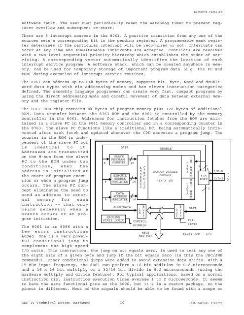
The 8361 ROM chip contains 8k bytes of program memory plus 128 bytes of additional<br />
RAM. Data transfer between the 8763 ROM and the 8061 is controlled by the memory<br />
controller in the 8061. Addresses for instruction fetches from the ROM are maintained<br />
in a slave PC in the 8061 memory controller and in a corresponding counter in<br />
the 8763. The slave PC functions like a traditional PC, being automatically incremented<br />
after each fetch and updated whenever the CPU executes a program jump. The<br />
counter in the ROM is inde-<br />
pendent of the slave PC but<br />
is identical to it.<br />
Addresses are transmitted<br />
on the M-bus from the slave<br />
PC to the ROM under two<br />
conditions, when the<br />
address is initialized at<br />
the start of program execution<br />
or when a program jump<br />
occurs. The slave PC concept<br />
eliminates the need to<br />
send an address to external<br />
memory for each<br />
instruction -- that only<br />
being necessary when a<br />
branch occurs or at program<br />
initiation.<br />
The 8061 is an 8096 with a<br />
few extra instructions<br />
added. One is a very powerful<br />
conditional jump to<br />
complement the high speed<br />
8<br />
8<br />
8<br />
DATA<br />
SLAVE<br />
PROGRAM<br />
COUNTER<br />
DATA<br />
ADDRESS<br />
REGISTER<br />
MACHINE<br />
STATE LOGIC<br />
RANDOM-ACCESS<br />
MEMORY<br />
(1K X 16)<br />
I/O units. This instruction, the jump on bit equals zero, is used to test any one of<br />
the eight bits of a given byte and jump if the bit equals zero (is this the JBC/JNB<br />
command?). Other conditional jumps were added to avoid extensive data shifts. With a<br />
15 MHz input frequency, the 8061 can perform a 16-bit addition in 0.8 microseconds<br />
and a 16 x 16 bit multiply or a 32/16 bit divide in 5.2 microseconds (using the<br />
hardware multiply and divide feature). For typical applications, based on a normal<br />
instruction mix, instruction execution times average 1 to 2 microseconds. It seems<br />
to have the same functional pins as the 8096, but it's in a custom package, so the<br />
pinout is different. Most of the signals should be able to be found with a scope or<br />
<strong>EEC</strong>-<strong>IV</strong> Technical Notes: Hardware 10 last edited: 9/29/98<br />
16<br />
EXECUTE<br />
ENABLE<br />
REGISTER 16<br />
ADDR/DATA<br />
16<br />
A<br />
D<br />
D<br />
R<br />
E<br />
S<br />
S<br />
C<br />
I<br />
R<br />
C<br />
U<br />
I<br />
T<br />
S<br />
B<br />
I U<br />
N F<br />
F<br />
C<strong>ON</strong>TROL<br />
SIGNALS<br />
MBUS<br />
MB0-MB7<br />
ENABLE<br />
B<br />
O U<br />
U F<br />
T F<br />
D<br />
A<br />
T<br />
A<br />
D<br />
A<br />
T<br />
A<br />
I<br />
N<br />
A<br />
S<br />
S<br />
Y<br />
O<br />
U<br />
T<br />
M<br />
U<br />
X<br />
DATA<br />
TRI-<br />
STATE<br />
8<br />
5<br />
I/O<br />
PORT<br />
5<br />
81C61 RAM - I/O<br />
I/O-0<br />
I/O-4<br />
I<br />
/<br />
O