TECHNICAL NOTES ON THE EEC-IV MCU - Auto diagnostics
TECHNICAL NOTES ON THE EEC-IV MCU - Auto diagnostics
TECHNICAL NOTES ON THE EEC-IV MCU - Auto diagnostics

You also want an ePaper? Increase the reach of your titles
YUMPU automatically turns print PDFs into web optimized ePapers that Google loves.
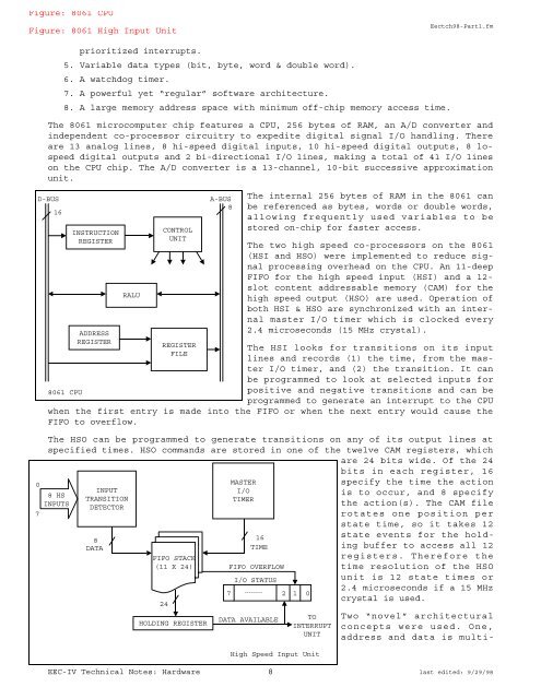
Figure: 8061 CPU<br />
Figure: 8061 High Input Unit<br />
prioritized interrupts.<br />
5. Variable data types (bit, byte, word & double word).<br />
6. A watchdog timer.<br />
7. A powerful yet “regular” software architecture.<br />
8. A large memory address space with minimum off-chip memory access time.<br />
Eectch98-Part1.fm<br />
The 8061 microcomputer chip features a CPU, 256 bytes of RAM, an A/D converter and<br />
independent co-processor circuitry to expedite digital signal I/O handling. There<br />
are 13 analog lines, 8 hi-speed digital inputs, 10 hi-speed digital outputs, 8 lospeed<br />
digital outputs and 2 bi-directional I/O lines, making a total of 41 I/O lines<br />
on the CPU chip. The A/D converter is a 13-channel, 10-bit successive approximation<br />
unit.<br />
D-BUS A-BUS<br />
16<br />
8<br />
0<br />
7<br />
8061 CPU<br />
INSTRUCTI<strong>ON</strong><br />
REGISTER<br />
ADDRESS<br />
REGISTER<br />
RALU<br />
C<strong>ON</strong>TROL<br />
UNIT<br />
REGISTER<br />
FILE<br />
The internal 256 bytes of RAM in the 8061 can<br />
be referenced as bytes, words or double words,<br />
allowing frequently used variables to be<br />
stored on-chip for faster access.<br />
The two high speed co-processors on the 8061<br />
(HSI and HSO) were implemented to reduce signal<br />
processing overhead on the CPU. An 11-deep<br />
FIFO for the high speed input (HSI) and a 12slot<br />
content addressable memory (CAM) for the<br />
high speed output (HSO) are used. Operation of<br />
both HSI & HSO are synchronized with an internal<br />
master I/O timer which is clocked every<br />
2.4 microseconds (15 MHz crystal).<br />
The HSI looks for transitions on its input<br />
lines and records (1) the time, from the master<br />
I/O timer, and (2) the transition. It can<br />
be programmed to look at selected inputs for<br />
positive and negative transitions and can be<br />
programmed to generate an interrupt to the CPU<br />
when the first entry is made into the FIFO or when the next entry would cause the<br />
FIFO to overflow.<br />
The HSO can be programmed to generate transitions on any of its output lines at<br />
specified times. HSO commands are stored in one of the twelve CAM registers, which<br />
are 24 bits wide. Of the 24<br />
8 HS<br />
INPUTS<br />
INPUT<br />
TRANSITI<strong>ON</strong><br />
DETECTOR<br />
8<br />
DATA<br />
FIFO STACK<br />
(11 X 24)<br />
24<br />
HOLDING REGISTER<br />
MASTER<br />
I/O<br />
TIMER<br />
16<br />
TIME<br />
FIFO OVERFLOW<br />
I/O STATUS<br />
7 2 1 0<br />
DATA AVAILABLE<br />
TO<br />
INTERRUPT<br />
UNIT<br />
High Speed Input Unit<br />
bits in each register, 16<br />
specify the time the action<br />
is to occur, and 8 specify<br />
the action(s). The CAM file<br />
rotates one position per<br />
state time, so it takes 12<br />
state events for the holding<br />
buffer to access all 12<br />
registers. Therefore the<br />
time resolution of the HSO<br />
unit is 12 state times or<br />
2.4 microseconds if a 15 MHz<br />
crystal is used.<br />
Two “novel” architectural<br />
concepts were used. One,<br />
address and data is multi-<br />
<strong>EEC</strong>-<strong>IV</strong> Technical Notes: Hardware 8 last edited: 9/29/98