Manual - E-LAB Computers
Manual - E-LAB Computers
Manual - E-LAB Computers

You also want an ePaper? Increase the reach of your titles
YUMPU automatically turns print PDFs into web optimized ePapers that Google loves.
UPP1-X In-Circuit Programmer with USB-2<br />
Chipcon<br />
Basics<br />
The UPP1-X firmware also supports the in-Circuit programmable ZigBee Chip family CC1110, CC2510 and<br />
CC2430 from TI-Chipcon. .<br />
With the creation of a new project for the CC2430 in addition to an existing Flash hexfile also the correct CPU<br />
must be selected (CC2430-F32, CC2430-F64 or CC2430-F128).<br />
The generated supply voltage for the target can be set between 2.7V and 3.6V if the programmer has to<br />
supply the target. A valid CPU clock must be selected, either 16MHz or 32MHz.<br />
There are no fuse bits but a lock bit block. The meaning of these lock bits can be found in the datasheet of the<br />
CC2430.<br />
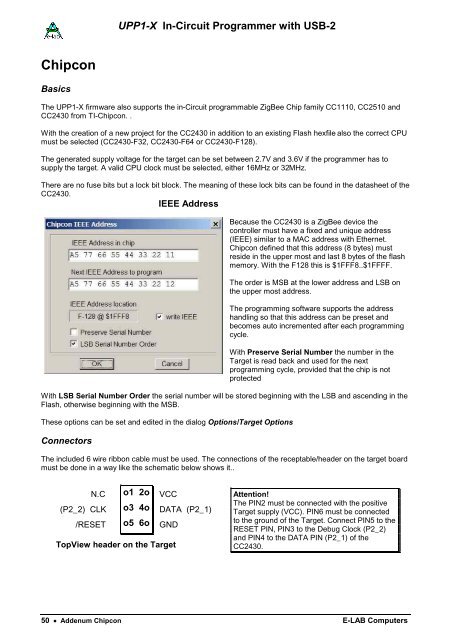
IEEE Address<br />
Because the CC2430 is a ZigBee device the<br />
controller must have a fixed and unique address<br />
(IEEE) similar to a MAC address with Ethernet.<br />
Chipcon defined that this address (8 bytes) must<br />
reside in the upper most and last 8 bytes of the flash<br />
memory. With the F128 this is $1FFF8..$1FFFF.<br />
The order is MSB at the lower address and LSB on<br />
the upper most address.<br />
The programming software supports the address<br />
handling so that this address can be preset and<br />
becomes auto incremented after each programming<br />
cycle.<br />
With Preserve Serial Number the number in the<br />
Target is read back and used for the next<br />
programming cycle, provided that the chip is not<br />
protected<br />
With LSB Serial Number Order the serial number will be stored beginning with the LSB and ascending in the<br />
Flash, otherwise beginning with the MSB.<br />
These options can be set and edited in the dialog Options/Target Options<br />
Connectors<br />
The included 6 wire ribbon cable must be used. The connections of the receptable/header on the target board<br />
must be done in a way like the schematic below shows it..<br />
N.C o1 2o VCC<br />
(P2_2) CLK o3 4o DATA (P2_1)<br />
/RESET o5 6o GND<br />
TopView header on the Target<br />
Attention!<br />
The PIN2 must be connected with the positive<br />
Target supply (VCC). PIN6 must be connected<br />
to the ground of the Target. Connect PIN5 to the<br />
RESET PIN, PIN3 to the Debug Clock (P2_2)<br />
and PIN4 to the DATA PIN (P2_1) of the<br />
CC2430.<br />
50 · Addenum Chipcon E-<strong>LAB</strong> <strong>Computers</strong>