T 7.2.1.3 Amplitude Modulation
T 7.2.1.3 Amplitude Modulation
T 7.2.1.3 Amplitude Modulation

You also want an ePaper? Increase the reach of your titles
YUMPU automatically turns print PDFs into web optimized ePapers that Google loves.
%<br />
0<br />
TPS <strong>7.2.1.3</strong><br />
Double Sideband AM<br />
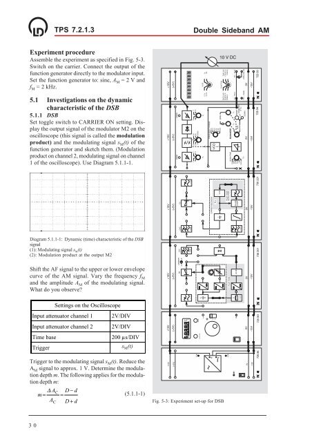
Experiment procedure<br />
Assemble the experiment as specified in Fig. 5-3.<br />
Switch on the carrier. Connect the output of the<br />
function generator directly to the modulator input.<br />
Set the function generator to: sine, A M = 2 V and<br />
f M = 2 kHz.<br />
5.1 Investigations on the dynamic<br />
characteristic of the DSB<br />
5.1.1 DSB<br />
Set toggle switch to CARRIER ON setting. Display<br />
the output signal of the modulator M2 on the<br />
oscilloscope (this signal is called the modulation<br />
product) and the modulating signal s M (t) of the<br />
function generator and sketch them. (<strong>Modulation</strong><br />
product on channel 2, modulating signal on channel<br />
1 of the oscilloscope). Use Diagram 5.1.1-1.<br />
GATE<br />
1s<br />
10s<br />
0,1s<br />
0,01s<br />
TIME A-B<br />
COUNT A<br />
CHECK<br />
FUNCTION<br />
RATIO A/B<br />
PERIOD A<br />
FREQ A<br />
TTL - IN(A) TTL - IN(A)<br />
ANALOG (A)<br />
TTL - IN(B)<br />
Diagram 5.1.1-1: Dynamic (time) characteristic of the DSB<br />
signal<br />
(1): Modulating signal s M<br />
(t)<br />
(2): <strong>Modulation</strong> product at the output M2<br />
Shift the AF signal to the upper or lower envelope<br />
curve of the AM signal. Vary the frequency f M<br />
and the amplitude A M of the modulating signal.<br />
What do you observe?<br />
Settings on the Oscilloscope<br />
Input attenuator channel 1<br />
Input attenuator channel 2<br />
2V/DIV<br />
2V/DIV<br />
kHz<br />
V pp<br />
=<br />
MODE<br />
OUT<br />
ATT<br />
dB<br />
20<br />
40<br />
TTL<br />
Time base<br />
Trigger<br />
200 µs/DIV<br />
s M (t)<br />
DC<br />
FUNCTION<br />
Trigger to the modulating signal s M (t). Reduce the<br />
A M signal to approx. 1 V. Determine the modulation<br />
depth m. The following applies for the modulation<br />
depth m:<br />
∆ A D d<br />
m = C −<br />
=<br />
(5.1.1-1)<br />
A D + d<br />
C<br />
+15V<br />
(+5V)<br />
I ><br />
U<br />
U<br />
Fig. 5-3: Experiment set-up for DSB<br />
I ><br />
M1<br />
0V<br />
30