Video and Image Processing Up Conversion Example Design
Video and Image Processing Up Conversion Example Design
Video and Image Processing Up Conversion Example Design

Create successful ePaper yourself
Turn your PDF publications into a flip-book with our unique Google optimized e-Paper software.
<strong>Video</strong> <strong>and</strong> <strong>Image</strong> <strong>Processing</strong> <strong>Up</strong> <strong>Conversion</strong> <strong>Example</strong> <strong>Design</strong><br />
Frame Buffer Component<br />
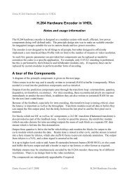
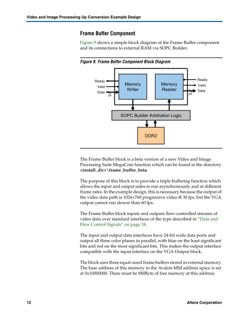
Figure 9 shows a simple block diagram of the Frame Buffer component<br />
<strong>and</strong> its connections to external RAM via SOPC Builder.<br />
Figure 9. Frame Buffer Component Block Diagram<br />
Ready<br />
Valid<br />
Data<br />
24<br />
Memory<br />
Writer<br />
Memory<br />
Reader<br />
SOPC Builder Arbitration Logic<br />
DDR2<br />
The Frame Buffer block is a beta version of a new <strong>Video</strong> <strong>and</strong> <strong>Image</strong><br />
<strong>Processing</strong> Suite MegaCore function which can be found in the directory<br />
\frame_buffer_beta.<br />
The purpose of this block is to provide a triple buffering function which<br />
allows the input <strong>and</strong> output sides to run asynchronously <strong>and</strong> at different<br />
frame rates. In the example design, this is necessary because the output of<br />
the video data path is 1024×768 progressive video @ 30 fps, but the VGA<br />
output cannot run slower than 60 fps.<br />
The Frame Buffer block inputs <strong>and</strong> outputs flow-controlled streams of<br />
video data over st<strong>and</strong>ard interfaces of the type described in “Data <strong>and</strong><br />
Flow Control Signals” on page 18.<br />
The input <strong>and</strong> output data interfaces have 24-bit wide data ports <strong>and</strong><br />
output all three color planes in parallel, with blue on the least significant<br />
bits <strong>and</strong> red on the most significant bits. This makes the output interface<br />
compatible with the input interface on the VGA Output block.<br />
The block uses three equal-sized frame buffers stored in external memory.<br />
The base address of this memory in the Avalon-MM address space is set<br />
at 0x10000000. There must be 8MByte of free memory at this address.<br />
12 Altera Corporation<br />
Preliminary<br />
24<br />
Ready<br />
Valid<br />
Data