201303.pdf 36567KB Mar 22 2013 09:11:22 PM
201303.pdf 36567KB Mar 22 2013 09:11:22 PM
201303.pdf 36567KB Mar 22 2013 09:11:22 PM

Create successful ePaper yourself
Turn your PDF publications into a flip-book with our unique Google optimized e-Paper software.
ent sink of approximately 400 mV is<br />
necessary. For a string of eight LEDs<br />
(where V F<br />
=8×3.2=25.6V), this results<br />
in a power loss of approximately 1.5%<br />
in I SINK<br />
. Without the offset cancellation<br />
included in the AMS backlight<br />
LED drivers, the value of V SET<br />
would be<br />
V REF<br />
V REF +<br />
R SET I LED<br />
−<br />
V SINK<br />
R SET<br />
higher, leading to higher power losses at<br />
the current sink.<br />
Power oPtimization<br />
As described earlier, a feedback path<br />
from the LED driver to the SMPS sets<br />
the drain voltage to the minimum<br />
I LED<br />
V SINK<br />
I LED<br />
I LED<br />
V SINK<br />
I LED I LED I LED<br />
V SINK V SINK V SINK V SINK<br />
(a) (b) (c) (d)<br />
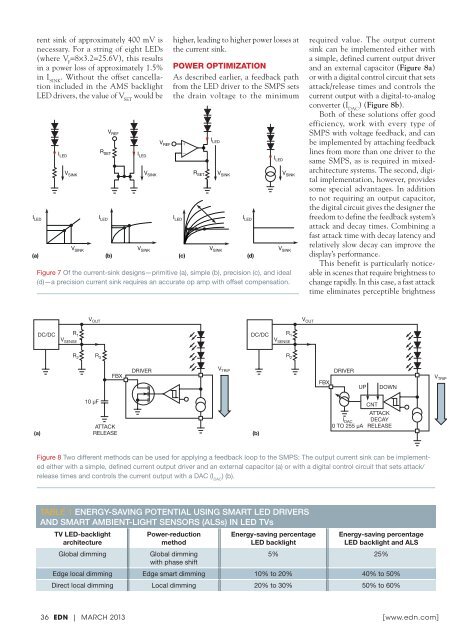
Figure 7 Of the current-sink designs—primitive (a), simple (b), precision (c), and ideal<br />
(d)—a precision current sink requires an accurate op amp with offset compensation.<br />
I LED<br />
V SINK<br />
required value. The output current<br />
sink can be implemented either with<br />
a simple, defined current output driver<br />
and an external capacitor (Figure 8a)<br />
or with a digital control circuit that sets<br />
attack/release times and controls the<br />
current output with a digital-to-analog<br />
converter (I DAC<br />
) (Figure 8b).<br />
Both of these solutions offer good<br />
efficiency, work with every type of<br />
SMPS with voltage feedback, and can<br />
be implemented by attaching feedback<br />
lines from more than one driver to the<br />
same SMPS, as is required in mixedarchitecture<br />
systems. The second, digital<br />
implementation, however, provides<br />
some special advantages. In addition<br />
to not requiring an output capacitor,<br />
the digital circuit gives the designer the<br />
freedom to define the feedback system’s<br />
attack and decay times. Combining a<br />
fast attack time with decay latency and<br />
relatively slow decay can improve the<br />
display’s performance.<br />
This benefit is particularly noticeable<br />
in scenes that require brightness to<br />
change rapidly. In this case, a fast attack<br />
time eliminates perceptible brightness<br />
DC/DC<br />
V OUT<br />
R 1<br />
V SENSE<br />
R 2 R 3<br />
FBX<br />
DRIVER<br />
EDN1303DF Fig 7.eps DIANE<br />
V TRIP<br />
DC/DC<br />
V OUT<br />
R 1<br />
V SENSE<br />
R 2<br />
FBX<br />
DRIVER<br />
V TRIP<br />
UP<br />
DOWN<br />
(a)<br />
10 µF<br />
ATTACK<br />
RELEASE<br />
(b)<br />
I DAC<br />
0 TO 255 µA<br />
CNT<br />
ATTACK<br />
DECAY<br />
RELEASE<br />
Figure 8 Two different methods can be used for applying a feedback loop to the SMPS: The output current sink can be implemented<br />
either with a simple, defined current output driver and an external capacitor (a) or with a digital control circuit that sets attack/<br />
release times and controls the current output with a DAC (I DAC<br />
) (b).<br />
TAble 1 EnErgy-saving potEntial using smart lED DrivErs<br />
anD smart ambiEnt-light sEnsors (alss) in lED tvs<br />
TV LED-backlight<br />
architecture<br />
Global dimming<br />
Power-reduction<br />
method<br />
Global dimming<br />
with phase shift<br />
Energy-saving percentage<br />
LED backlight<br />
Energy-saving percentage<br />
LED backlight and ALS<br />
5% 25%<br />
edge local dimming edge smart dimming 10% to 20% 40% to 50%<br />
Direct local dimming local dimming 20% to 30% 50% to 60%<br />
EDN1303DF Fig 8.eps DIANE<br />
36 EDN | MARCH <strong>2013</strong> [ www.edn.com ]


![[270].pdf 37407KB Sep 02 2010 09:55:57 AM - ElectronicsAndBooks](https://img.yumpu.com/50350834/1/185x260/270pdf-37407kb-sep-02-2010-095557-am-electronicsandbooks.jpg?quality=85)
![draaien, A Viruly 1935 OCR c20130324 [320]. - ElectronicsAndBooks](https://img.yumpu.com/49957773/1/190x252/draaien-a-viruly-1935-ocr-c20130324-320-electronicsandbooks.jpg?quality=85)


![20051110 c20051031 [105].pdf 35001KB Feb 18 2009 08:46:32 PM](https://img.yumpu.com/48687202/1/190x253/20051110-c20051031-105pdf-35001kb-feb-18-2009-084632-pm.jpg?quality=85)