201303.pdf 36567KB Mar 22 2013 09:11:22 PM
201303.pdf 36567KB Mar 22 2013 09:11:22 PM
201303.pdf 36567KB Mar 22 2013 09:11:22 PM

You also want an ePaper? Increase the reach of your titles
YUMPU automatically turns print PDFs into web optimized ePapers that Google loves.
designideas<br />
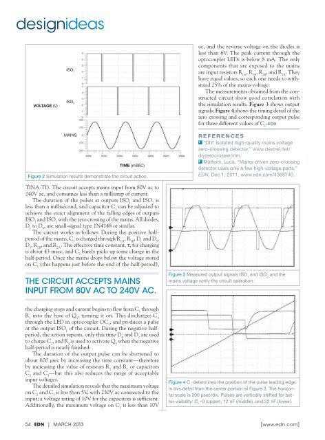
VOLTAGE (V)<br />
ISO 1<br />
ISO 2<br />
ac, and the reverse voltage on the diodes is<br />
less than 6V. The peak current through the<br />
optocoupler LEDs is below 8 mA. The only<br />
components that are exposed to the mains<br />
are input resistors R 1A<br />
, R 1B<br />
, R 2B<br />
, and R 2B<br />
. They<br />
have equal values, so each one needs to withstand<br />
25% of the mains voltage.<br />
The measurements obtained from the constructed<br />
circuit show good correlation with<br />
the simulation results. Figure 3 shows output<br />
signals; Figure 4 shows the timing detail of the<br />
zero crossing and corresponding output pulse<br />
for three different values of C 1<br />
.EDN<br />
MAINS<br />
TIME (mSEC)<br />
Figure 2 Simulation results demonstrate the circuit action.<br />
RefeR ences<br />
1 “DIY: Isolated high-quality mains voltage<br />
zero-crossing detector,” www.dextrel.net/<br />
diyzerocrosser.htm.<br />
2 Matteini, Luca, “Mains-driven zero-crossing<br />
detector uses only a few high-voltage parts,”<br />
EDN, Dec 1, 20<strong>11</strong>, www.edn.com/4368740.<br />
TINA-TI). The circuit accepts mains input from 80V ac to<br />
240V ac, and consumes less than a milliamp of current.<br />
The duration of the pulses at outputs ISO 1<br />
and ISO 2<br />
is<br />
less than a millisecond, and capacitor C 1<br />
can be adjusted to<br />
achieve the exact alignment of the falling edges of outputs<br />
ISO 1<br />
and ISO 2<br />
with the zero crossing of the mains. All diodes,<br />
D 1<br />
to D 5<br />
, are small-signal type 1N4148 or similar.<br />
The circuit works as follows: During the positive halfperiod<br />
of the mains, C 3<br />
is charged through R 1A<br />
, R 1B<br />
, D 1<br />
and D 5<br />
,<br />
D 3<br />
, R 2B<br />
, and R 2A<br />
. The effective time constant, τ, for charging<br />
is about 43 msec, and C 3<br />
barely picks up some charge in the<br />
half-period. Once the mains drops below the voltage stored<br />
on C 3<br />
(this happens just before the end of the half-period),<br />
The circuiT accepTs mains<br />
inpuT from 80V ac To 240V ac.<br />
Figure 3 Measured output signals ISO 1<br />
and ISO 2<br />
and the<br />
mains voltage verify the circuit operation.<br />
the charging stops and current begins to flow from C 3<br />
through<br />
R 3<br />
into the base of Q 5<br />
, turning it on. This discharges C 3<br />
through the LED in optocoupler OC 1<br />
, and produces a pulse<br />
at the output ISO 1<br />
of the circuit. During the negative halfperiod,<br />
the action repeats, only this time D 4<br />
and D 2<br />
are used<br />
to charge C 2<br />
, and R 4<br />
is used to activate Q 5<br />
when the negative<br />
half-period is nearly finished.<br />
The duration of the output pulse can be shortened to<br />
about 600 μsec by increasing the time constant—therefore<br />
by increasing the value of resistors R 1<br />
and R 2<br />
or capacitors<br />
C 2<br />
and C 3<br />
—but this also reduces the range of acceptable<br />
input voltages.<br />
The detailed simulation reveals that the maximum voltage<br />
on C 2<br />
and C 3<br />
is less than 5V, with 250V ac connected to the<br />
input; a voltage rating of 10V for the capacitors is sufficient.<br />
Additionally, the maximum voltage on C 1<br />
is less than 10V<br />
Figure 4 C 1<br />
determines the position of the pulse leading edge<br />
in this detail from the center portion of Figure 3. The horizontal<br />
scale is 200 µsec/div. Pulses are vertically shifted for better<br />
visibility: C 1<br />
=0 (upper), 12 nF (middle), and <strong>22</strong> nF (lower).<br />
54 EDN | <strong>Mar</strong>ch <strong>2013</strong> [ www.edn.com ]


![[270].pdf 37407KB Sep 02 2010 09:55:57 AM - ElectronicsAndBooks](https://img.yumpu.com/50350834/1/185x260/270pdf-37407kb-sep-02-2010-095557-am-electronicsandbooks.jpg?quality=85)
![draaien, A Viruly 1935 OCR c20130324 [320]. - ElectronicsAndBooks](https://img.yumpu.com/49957773/1/190x252/draaien-a-viruly-1935-ocr-c20130324-320-electronicsandbooks.jpg?quality=85)


![20051110 c20051031 [105].pdf 35001KB Feb 18 2009 08:46:32 PM](https://img.yumpu.com/48687202/1/190x253/20051110-c20051031-105pdf-35001kb-feb-18-2009-084632-pm.jpg?quality=85)