201303.pdf 36567KB Mar 22 2013 09:11:22 PM
201303.pdf 36567KB Mar 22 2013 09:11:22 PM
201303.pdf 36567KB Mar 22 2013 09:11:22 PM

Create successful ePaper yourself
Turn your PDF publications into a flip-book with our unique Google optimized e-Paper software.
designideas<br />
readerS SOLVe deSIGN PrOBLeMS<br />
Circuit maximizes pulse-widthmodulated<br />
DAC throughput<br />
Ajoy Raman, Bangalore, India<br />
↘<br />
Simple DACs realized by lowpass<br />
filtering microcontrollergenerated<br />
pulse-width-modulated<br />
(PWM) signals have a response that is<br />
typically a tenth of the PWM frequency.<br />
This Design Idea is a novel implementation<br />
of a previously published<br />
method 1 employing a reference ramp<br />
whose output is sampled and held by<br />
the PWM signal. This approach results<br />
in a throughput rate equal to the PWM<br />
frequency.<br />
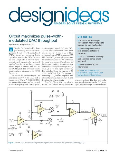
You can use the circuit in Figure 1 to<br />
implement a ±10V 10-bit DAC with a<br />
throughput of 20 kHz. A DSPIC30F40<strong>11</strong><br />
microcontroller (not shown) is operated<br />
at a clock frequency of 96 MHz to generate<br />
the capture signals OC 1<br />
and OC 4<br />
.<br />
Clock/4 is fed to an internal 16-bit timer<br />
whose period is set for a count of 1200<br />
corresponding to a PWM frequency of 20<br />
kHz. Signal OC 4<br />
is mostly high and goes<br />
low at a fixed count of <strong>11</strong>70 as a reference<br />
for ramp generation. IC 1A<br />
, along with<br />
Q 1<br />
, forms a precision constant-current<br />
source that linearly charges capacitor C 2<br />
when Q 2<br />
is off. This signal inverted by<br />
IC 3A<br />
switches Q 2<br />
on for a period of 30<br />
counts to discharge C 2<br />
for the start of the<br />
next ramp. IC 1B<br />
buffers, amplifies, and<br />
offsets the ramp; potentiometers R 2<br />
and<br />
R 5<br />
adjust the offset and gain.<br />
The OC 1<br />
falling edge controls the<br />
PWM DAC sample timing relative to<br />
DIs Inside<br />
52 A circuit for mains synchronization<br />
has two separate<br />
outputs for each half-period<br />
55 Low-component-count<br />
zero-crossing detector is<br />
low power<br />
57 DC-DC converter starts up<br />
and operates from a single<br />
photocell<br />
58 Filter quashes 60-Hz<br />
interference<br />
▶To see and comment on<br />
all of EDN’s Design Ideas, visit<br />
www.edn.com/designideas.<br />
the ramp voltage. The data word to be<br />
converted determines the OC 1<br />
duty<br />
cycle by comparing it internally in the<br />
15V<br />
15V<br />
5V<br />
R 1<br />
2.7k<br />
R 2<br />
1k<br />
R 3<br />
18k<br />
–15V<br />
R 4<br />
56k<br />
PIN 19<br />
OC 4<br />
1<br />
OUTPUTS<br />
FROM<br />
DSPIC30F40<strong>11</strong><br />
14<br />
5V<br />
7<br />
C 3<br />
680 pF<br />
R 9<br />
1.8k<br />
R 5<br />
10k<br />
R 7<br />
18k<br />
IC 3A<br />
CD40106<br />
5V<br />
2 4<br />
−<br />
IC 1A<br />
LF353<br />
3<br />
+<br />
8<br />
15V<br />
R 8<br />
2.2k<br />
IC 3B<br />
CD40106<br />
PIN 23<br />
3<br />
4<br />
OC 1<br />
2<br />
1<br />
Q 1<br />
BC177<br />
Q 2<br />
BC107<br />
R 6<br />
1k<br />
C 2<br />
0.1 μF<br />
MYLAR<br />
6<br />
−<br />
IC 1B<br />
LF353<br />
5<br />
+<br />
7<br />
ANALOG IN<br />
S/H IN<br />
15V<br />
3<br />
1 2<br />
IC 2<br />
LF398<br />
8<br />
4 7 6<br />
–15V<br />
5<br />
C 1<br />
1800 pF<br />
DAC<br />
OUTPUT<br />
Figure 1 The off-page microcontroller generates signals for ramp control (OC 4<br />
) and sample timing (OC 1<br />
).<br />
[ www.edn.com ] <strong>Mar</strong>ch <strong>2013</strong> | EDN 51


![[270].pdf 37407KB Sep 02 2010 09:55:57 AM - ElectronicsAndBooks](https://img.yumpu.com/50350834/1/185x260/270pdf-37407kb-sep-02-2010-095557-am-electronicsandbooks.jpg?quality=85)
![draaien, A Viruly 1935 OCR c20130324 [320]. - ElectronicsAndBooks](https://img.yumpu.com/49957773/1/190x252/draaien-a-viruly-1935-ocr-c20130324-320-electronicsandbooks.jpg?quality=85)


![20051110 c20051031 [105].pdf 35001KB Feb 18 2009 08:46:32 PM](https://img.yumpu.com/48687202/1/190x253/20051110-c20051031-105pdf-35001kb-feb-18-2009-084632-pm.jpg?quality=85)