201303.pdf 36567KB Mar 22 2013 09:11:22 PM
201303.pdf 36567KB Mar 22 2013 09:11:22 PM
201303.pdf 36567KB Mar 22 2013 09:11:22 PM

Create successful ePaper yourself
Turn your PDF publications into a flip-book with our unique Google optimized e-Paper software.
designideas<br />
ANALOG<br />
SIGNALS<br />
DIGITAL<br />
SIGNALS<br />
10<br />
0<br />
–10<br />
H<br />
DAC OUTPUT<br />
H L H L OC 4 PWM REF<br />
L<br />
0 10 20 30 40 50 60 70 80 90 100<br />
TIME (μSEC)<br />
microcontroller with the internal 16-bit<br />
timer. C 3<br />
and R 9<br />
differentiate the resulting<br />
PWM signal; IC 3B<br />
then inverts it,<br />
forming a 1-μsec sample signal for the<br />
sample-and-hold IC 2<br />
. Pin 5 of IC 2<br />
forms<br />
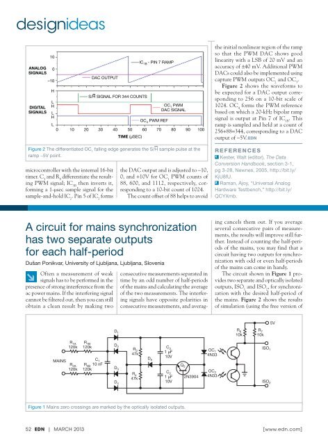
S/H SIGNAL FOR 344 COUNTS<br />
IC 1B - PIN 7 RAMP<br />
OC 1 PWM<br />
DAC SIGNAL<br />
Figure 2 The differentiated OC 1<br />
falling edge generates the S/H sample pulse at the<br />
ramp −5V point.<br />
the DAC output and is adjusted to −10,<br />
0, and +10V for OC 1<br />
PWM counts of<br />
88, 600, and <strong>11</strong>12, respectively, corresponding<br />
to a 10-bit count of 1024.<br />
The count offset of 88 helps to avoid<br />
the initial nonlinear region of the ramp<br />
so that the PWM DAC shows good<br />
linearity with a LSB of 20 mV and an<br />
accuracy of ±40 mV. Additional PWM<br />
DACs could also be implemented using<br />
capture PWM outputs OC 2<br />
and OC 3<br />
.<br />
Figure 2 shows the waveforms to<br />
be expected for a DAC output corresponding<br />
to 256 on a 10-bit scale of<br />
1024. OC 4<br />
forms the PWM reference<br />
based on which a 20-kHz bipolar ramp<br />
signal is output at Pin 7 of IC 1B<br />
. This<br />
ramp is sampled and held at a count of<br />
256+88=344, corresponding to a DAC<br />
output of −5V. EDN<br />
RefeR ences<br />
1 Kester, Walt (editor), The Data<br />
Conversion Handbook, section 3-1,<br />
pg 3-28, Newnes, 2005, http://bit.ly/<br />
KjU8fU.<br />
2 Raman, Ajoy, “Universal Analog<br />
Hardware Testbench,” http://bit.ly/<br />
QCYXmb.<br />
A circuit for mains synchronization<br />
has two separate outputs<br />
for each half-period<br />
EDNDI5324 Fig 2.eps DIANE<br />
Dušan Ponikvar, University of Ljubljana, Ljubljana, Slovenia<br />
↘<br />
Often a measurement of weak<br />
signals has to be performed in the<br />
presence of strong interference from the<br />
ac power mains. If the interfering signal<br />
cannot be filtered out, then you can still<br />
obtain a clean result by making two<br />
consecutive measurements separated in<br />
time by an odd number of half-periods<br />
of the mains and calculating the average<br />
of the two measurements. The interfering<br />
signals have opposite polarities in<br />
consecutive measurements, and averaging<br />
cancels them out. If you average<br />
several consecutive pairs of measurements,<br />
the results will improve still further.<br />
Instead of counting the half-periods<br />
of the mains, you may find that a<br />
circuit having two outputs for synchronization<br />
with odd or even half-periods<br />
of the mains can come in handy.<br />
The circuit shown in Figure 1 provides<br />
two separate and optically isolated<br />
outputs, ISO 1<br />
and ISO 2<br />
, for synchronization<br />
with the desired half-period of<br />
the mains. Figure 2 shows the results<br />
of simulation (using the free version of<br />
MAINS<br />
R 1A<br />
120k<br />
R 2A<br />
120k<br />
R 1B<br />
120k<br />
C 1<br />
R 2B 10 nF<br />
120k<br />
D 1<br />
D 2<br />
D 3<br />
D 4<br />
R 3<br />
47k<br />
R 4<br />
47k<br />
D 5<br />
C 3<br />
1 μF<br />
10V<br />
C 2<br />
1 μF<br />
10V<br />
Q 5<br />
2N3904<br />
OC 1<br />
4N33<br />
OC 2<br />
4N33<br />
R 6<br />
10k<br />
5V<br />
R 7<br />
10k<br />
ISO 1<br />
ISO 2<br />
Figure 1 Mains zero crossings are marked by the optically isolated outputs.<br />
52 EDN | <strong>Mar</strong>ch <strong>2013</strong> [ www.edn.com ]


![[270].pdf 37407KB Sep 02 2010 09:55:57 AM - ElectronicsAndBooks](https://img.yumpu.com/50350834/1/185x260/270pdf-37407kb-sep-02-2010-095557-am-electronicsandbooks.jpg?quality=85)
![draaien, A Viruly 1935 OCR c20130324 [320]. - ElectronicsAndBooks](https://img.yumpu.com/49957773/1/190x252/draaien-a-viruly-1935-ocr-c20130324-320-electronicsandbooks.jpg?quality=85)


![20051110 c20051031 [105].pdf 35001KB Feb 18 2009 08:46:32 PM](https://img.yumpu.com/48687202/1/190x253/20051110-c20051031-105pdf-35001kb-feb-18-2009-084632-pm.jpg?quality=85)