201303.pdf 36567KB Mar 22 2013 09:11:22 PM
201303.pdf 36567KB Mar 22 2013 09:11:22 PM
201303.pdf 36567KB Mar 22 2013 09:11:22 PM

You also want an ePaper? Increase the reach of your titles
YUMPU automatically turns print PDFs into web optimized ePapers that Google loves.
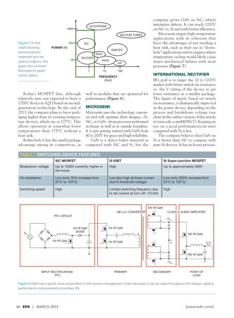
Figure 7 In this<br />
chart showing<br />
semiconductor<br />
materials and frequency<br />
regions, the<br />
green box outlines<br />
Microsemi’s application<br />
space.<br />
1000<br />
100<br />
POWER (W)<br />
10<br />
Rohm’s MOSFET line, although<br />
relatively new, was expected to have a<br />
1700V device in 1Q13 based on secondgeneration<br />
technology. By the end of<br />
<strong>2013</strong>, the company plans to have packaging<br />
higher than its existing temperature<br />
devices, which are at 175°C. This<br />
allows operation at somewhat lower<br />
temperatures than 175°C without a<br />
heat sink.<br />
Rohm feels it has the small-package<br />
advantage among its competitors, as<br />
SiC<br />
SILICON<br />
KLYSTRONS<br />
SiGe<br />
AsGa<br />
GaN/SiC<br />
VACUUM TUBES<br />
InP<br />
1 10 100<br />
FREQUENCY<br />
(GHz)<br />
well as modules that are optimized for<br />
performance (Figure 6).<br />
MicroseMi<br />
Microsemi uses the technology customers<br />
feel will optimize their designs—Si,<br />
SiC, or GaN—from processes performed<br />
in-house as well as at outside foundries.<br />
It is just getting started with GaN from<br />
EDN1303CS Fig 14.eps DIANE<br />
40 to 200V for space and high reliability.<br />
GaN is a defect-laden material as<br />
compared with SiC and Si, but the<br />
company grows GaN on SiC, which<br />
minimizes defects. It can reach 1200V<br />
on SiC vs. Si and with better efficiency.<br />
Microsemi targets high-temperature<br />
applications with its solutions that<br />
have the advantages of not needing a<br />
heat sink, such as their use in “downhole”<br />
applications and in engines where<br />
temperature cycling would likely cause<br />
major mechanical failures with most<br />
processes (Figure 7).<br />
international rectifier<br />
IR’s goal is to target the 20 to 1200V<br />
market with better switch on-resistance<br />
vs. the V rating of the device to get<br />
lower resistance in a smaller package.<br />
The figure of merit, based on switch<br />
on-resistance, is dramatically improved<br />
in the power device, depending on the<br />
process and breakdown voltage (see<br />
chart in the online version of this article<br />
at www.edn.com/44<strong>09</strong>627). Keeping an<br />
eye on a good performance/cost ratio<br />
compared with Si is key.<br />
The company believes that GaN on<br />
Si is better than SiC to compete with<br />
pure-Si devices. It has in-house process-<br />
Table 1 Switching-device featureS<br />
SiC MOSFET Si IGBT Si Super-junction MOSFET<br />
breakdown voltage Up to 1200V currently; higher in<br />
the future<br />
High<br />
Up to approximately 900V<br />
On-resistance<br />
low (only 35% increase from<br />
25°C to 150°C)<br />
low (but high at lower current<br />
due to threshold voltage)<br />
low (only 250% increase from<br />
25°C to 150°C)<br />
Switching speed High limited switching frequency due<br />
to tail current at turn-off


![[270].pdf 37407KB Sep 02 2010 09:55:57 AM - ElectronicsAndBooks](https://img.yumpu.com/50350834/1/185x260/270pdf-37407kb-sep-02-2010-095557-am-electronicsandbooks.jpg?quality=85)
![draaien, A Viruly 1935 OCR c20130324 [320]. - ElectronicsAndBooks](https://img.yumpu.com/49957773/1/190x252/draaien-a-viruly-1935-ocr-c20130324-320-electronicsandbooks.jpg?quality=85)


![20051110 c20051031 [105].pdf 35001KB Feb 18 2009 08:46:32 PM](https://img.yumpu.com/48687202/1/190x253/20051110-c20051031-105pdf-35001kb-feb-18-2009-084632-pm.jpg?quality=85)