201303.pdf 36567KB Mar 22 2013 09:11:22 PM
201303.pdf 36567KB Mar 22 2013 09:11:22 PM
201303.pdf 36567KB Mar 22 2013 09:11:22 PM

You also want an ePaper? Increase the reach of your titles
YUMPU automatically turns print PDFs into web optimized ePapers that Google loves.
Designing a power backup system is easy with the<br />
LTC3<strong>22</strong>6. For example, take a device that has an operating<br />
current of 150mA and a standby current (I SB ) of 50mA<br />
when powered from a single-cell Li-Ion battery. To ensure<br />
that a charged battery is present, the power-fail comparator<br />
(PFI) high trigger point is set to 3.6V. The device enters<br />
standby mode when the battery voltage reaches 3.15V<br />
and enters backup mode at 3.10V (V BAT(MIN) ), initializing<br />
holdup power for a time period (t HU ) of about 45 seconds.<br />
The standby mode trigger level is controlled by an external<br />
comparator circuit while the backup mode trigger level<br />
is controlled by the PFI comparator. While in backup<br />
mode, the device must be inhibited from entering full<br />
operational mode to prevent overly fast discharge of the<br />
supercapacitors.<br />
The design begins by setting the PFI trigger level. R2 is<br />
set at 121k and R1 is calculated to set the PFI trigger level<br />
at the PFI pin (V PFI ) to 1.2V.<br />
R1= V BAT(MIN) –V PFI<br />
V PFI<br />
Data Sheet Download<br />
www.linear.com<br />
•R2= 191.6kΩ<br />
Set R1 to 191k.<br />
The hysteresis on the V IN pin needs to be extended to<br />
meet the 3.6V trigger level. This can be accomplished by<br />
adding a series combination of a resistor and diode from<br />
the PFI pin to the PFO pin. V IN(HYS) is 0.5V, V PFI(HYS) is<br />
20mV and V f is 0.4V.<br />
V PFI + V PFI(HYS) –V f<br />
R8 =<br />
V IN(HYS) – V •R1= 349.3kΩ<br />
PFI(HYS)<br />
•(R1+R2)<br />
R2<br />
Set R8 to 348k.<br />
Set the LDO backup mode output voltage to 3.3V by<br />
setting R7 to 80.6k and calculating R6. V LDO(FB) is 0.8V.<br />
R6 = V OUT –V LDO(FB)<br />
V LDO(FB)<br />
•R7= 251.9kΩ<br />
Set R6 to 255k.<br />
The fully charged voltage on the series-connected<br />
supercapacitors is set to 5V. This is accomplished with<br />
a voltage divider network between the CPO pin and the<br />
CPO_FB pin. R5 is set to 1.21M and R4 is calculated.<br />
V CPO(FB) is 1.21V.<br />
R4= V CPO –V CPO(FB)<br />
V CPO(FB)<br />
•R5= 3.78MΩ<br />
Let R4 equal 3.83M.<br />
As the voltage on the supercapacitor stack starts to<br />
approach V OUT in backup mode, the ESR of the two<br />
supercapacitors and the output resistance of the LDO<br />
must be accounted for in the calculation of the minimum<br />
voltage on the supercapacitors at the end of t HU . Assume<br />
that the ESR of each supercapacitor is 100mΩ and the<br />
LDO output resistance is 200mΩ, which results in an<br />
additional 20mV to V OUT(MIN) due to the 50mA standby<br />
current. V OUT(MIN) is set to 3.1V, resulting in a discharge<br />
voltage (ΔV SCAP ) of 1.88V on the supercapacitor stack.<br />
The size of each supercapacitor can now be determined.<br />
C SCAP = 2• I SB •t HU<br />
ΔV SCAP<br />
= 2.39F<br />
Each supercapacitor is chosen to be a 3F/2.7V capacitor<br />
from Nesscap (ESHSR-0003C0-002R7).<br />
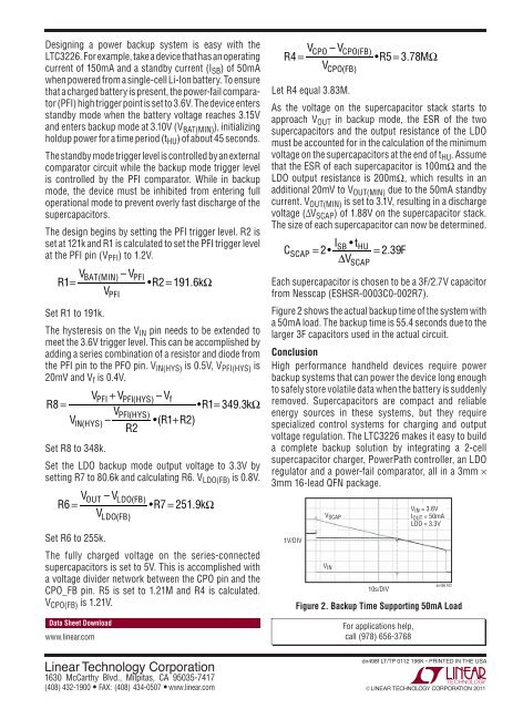
Figure 2 shows the actual backup time of the system with<br />
a 50mA load. The backup time is 55.4 seconds due to the<br />
larger 3F capacitors used in the actual circuit.<br />
Conclusion<br />
High performance handheld devices require power<br />
backup systems that can power the device long enough<br />
to safely store volatile data when the battery is suddenly<br />
removed. Supercapacitors are compact and reliable<br />
energy sources in these systems, but they require<br />
specialized control systems for charging and output<br />
voltage regulation. The LTC3<strong>22</strong>6 makes it easy to build<br />
a complete backup solution by integrating a 2-cell<br />
supercapacitor charger, PowerPath controller, an LDO<br />
regulator and a power-fail comparator, all in a 3mm ×<br />
3mm 16-lead QFN package.<br />
1V/DIV<br />
V SCAP<br />
V IN = 3.6V<br />
I OUT = 50mA<br />
LDO = 3.3V<br />
V IN<br />
10s/DIV<br />
Figure 2. Backup Time Supporting 50mA Load<br />
For applications help,<br />
call (978) 656-3768<br />
dn498 F02<br />
Linear Technology Corporation<br />
1630 McCarthy Blvd., Milpitas, CA 95035-7417<br />
(408) 432-1900 ● FAX: (408) 434-0507 ● www.linear.com<br />
dn498f LT/TP 0<strong>11</strong>2 196K • PRINTED IN THE USA<br />
© LINEAR TECHNOLOGY CORPORATION 20<strong>11</strong>


![[270].pdf 37407KB Sep 02 2010 09:55:57 AM - ElectronicsAndBooks](https://img.yumpu.com/50350834/1/185x260/270pdf-37407kb-sep-02-2010-095557-am-electronicsandbooks.jpg?quality=85)
![draaien, A Viruly 1935 OCR c20130324 [320]. - ElectronicsAndBooks](https://img.yumpu.com/49957773/1/190x252/draaien-a-viruly-1935-ocr-c20130324-320-electronicsandbooks.jpg?quality=85)


![20051110 c20051031 [105].pdf 35001KB Feb 18 2009 08:46:32 PM](https://img.yumpu.com/48687202/1/190x253/20051110-c20051031-105pdf-35001kb-feb-18-2009-084632-pm.jpg?quality=85)