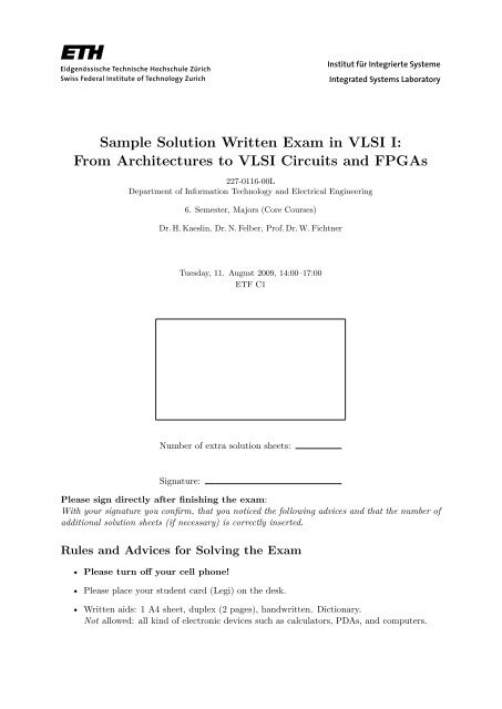
Sample Solution Written Exam in VLSI I - Integrated Systems ...
Sample Solution Written Exam in VLSI I - Integrated Systems ...
Sample Solution Written Exam in VLSI I - Integrated Systems ...

Create successful ePaper yourself
Turn your PDF publications into a flip-book with our unique Google optimized e-Paper software.
(b) On which part of the <strong>VLSI</strong> design flow where the practical exercises of the <strong>VLSI</strong> 1 ( 1 / 2 )lecture based on? Select the correct answer.A. Front-end design B. Back-end design(c) Select for each statement whether it is true or false.i) Logic simulation, tim<strong>in</strong>g verification and electrical rule check (ERC) are used ( 1 / 2 )to validate gate-level schematics or net lists.A. True B. Falseii) Design for test (DFT) allows the improvement of the controllability and observabilityof the <strong>in</strong>ner circuit nodes without add<strong>in</strong>g auxiliary( 1 / 2 )circuitry.A. True B. Falseiii) In the floor plann<strong>in</strong>g step, each cell is assigned to a specific location. After ( 1 / 2 )that the metal wires, carry<strong>in</strong>g the electrical signals between the cells, aredef<strong>in</strong>ed.A. True B. Falseiv) Layout versus schematic (LVS) verifies the conformity of the layout with geometricrules given by the technology( 1 / 2 )used.A. True B. FalseProblem 3: Field-programmable logic(a) Encircle the correct characteristic <strong>in</strong> each cell of the table.(3)Configuration Non- Reconfi- Unlimited Radiationtechnology volatile gurable endurance toleranceSRAM yes / no <strong>in</strong> / out yes / no good / poorof circuitEPROM yes / no <strong>in</strong> / out yes / no good / poorof circuitEEPROM yes / no <strong>in</strong> / out yes / no good / poorof circuit(b) The organization of hardware resources of field-programmable logic can be divided<strong>in</strong>to two classes: complex programmable logic devices (CPLD) and fieldprogrammablegate arrays (FPGA).Select for each statement whether it is true for CPLDs, for FPGAs or for both.i) This class(es) consist of many simple programmable logic devices.( 1 / 2 )A. CPLD B. FPGAPage 2 of 30<strong>VLSI</strong> I <strong>Exam</strong> Summer 2009
ii) The logic AND-operation between two 10-bit <strong>in</strong>put vectors can be realized <strong>in</strong> ( 1 / 2 )general with:A. CPLD B. FPGAiii) Which class of devices is better suited to realize a prototype for the upcom<strong>in</strong>g ( 1 / 2 )WirelessHD standard?A. CPLD B. FPGAiv) Look-up tables and switch boxes can be found <strong>in</strong>( 1 / 2 )A. CPLD B. FPGAv) What is the difference between a f<strong>in</strong>e-gra<strong>in</strong>ed FPGA architecture and a coarsegra<strong>in</strong>edFPGA(1)architecture?vi) The follow<strong>in</strong>g figures, Fig. 1, Fig. 2, and Fig. 3, each shows a logic cell of (1 1 / 2 )an FPGA family. Please note for each logic cell whether it is a f<strong>in</strong>e-gra<strong>in</strong>edarchitecture or a coarse-gra<strong>in</strong>ed architecture.The adaptive logic module cell shown <strong>in</strong> Fig. 1 belongs to aA. f<strong>in</strong>e-gra<strong>in</strong>ed architecture B. coarse-gra<strong>in</strong>ed architectureThe VersaTile cell <strong>in</strong> Fig. 2 of an Actel FPGA belongs to aA. f<strong>in</strong>e-gra<strong>in</strong>ed architecture B. coarse-gra<strong>in</strong>ed architectureThe Virtex-4 slice <strong>in</strong> Fig. 3 of a Xil<strong>in</strong>x FPGA belongs to aA. f<strong>in</strong>e-gra<strong>in</strong>ed architecture B. coarse-gra<strong>in</strong>ed architecturePage 3 of 30<strong>VLSI</strong> I <strong>Exam</strong> Summer 2009
Figure 1: An adaptive logic module of a Altera FPGAFigure 2: A logic VersaTile cell of an Actel FPGA.Page 4 of 30<strong>VLSI</strong> I <strong>Exam</strong> Summer 2009
Figure 3: A Virtex-4 slice of a Xil<strong>in</strong>x FPGAPage 5 of 30<strong>VLSI</strong> I <strong>Exam</strong> Summer 2009
2 From Algorithms to Architectures . . . . . . . . . . . . . . . . (50 po<strong>in</strong>ts)Problem 1: Decide whether the follow<strong>in</strong>g statements are correct. Give a short explanation for yourdecision.(a) The user <strong>in</strong>terface of a mobile phone is better implemented us<strong>in</strong>g dedicated hardware<strong>in</strong>stead of general purpose hardware to meet the str<strong>in</strong>gent low-power require-(1 1 / 2 )ments.(b) The video decoder of a DVD player is preferably implemented us<strong>in</strong>g ASIPs rather (1 1 / 2 )than dedicated hardware if the flexibility to quickly support new encod<strong>in</strong>g standardsis more important than area and power efficiency.(c) A data dependency graph does not allow any circular paths of weight zero. (1 1 / 2 )(d) The AT-product can not be significantly reduced when the architecture is transformedus<strong>in</strong>g iterative(1 1 / 2 )decomposition.(e) Coarse-gra<strong>in</strong>ed pipel<strong>in</strong><strong>in</strong>g can reduce the power consumption of a circuit.(1 1 / 2 )(f) Even for very small memories the area can be significantly reduced when the (1 1 / 2 )implementation is changed from registers to on-chip DRAM.Page 6 of 30<strong>VLSI</strong> I <strong>Exam</strong> Summer 2009
(a) Iterative architecturei) Draw a block diagram of the iterative algorithm. In each clock cycle, one (4)CORDIC iteration should be computed. The control path (<strong>in</strong>clud<strong>in</strong>g the calculationof d i ) can be neglected. Use only blocks given <strong>in</strong> Fig. 5. x(0), y(0), z(0)are the <strong>in</strong>puts of your circuit and x(N), y(N), z(N) the outputs after N iterations.ii) Calculate area, maximum frequency, and latency of this architecture for N=3 (2)iterations (all tim<strong>in</strong>g parameters not given <strong>in</strong> Fig. 5 are negligible).iii) Assume one pipel<strong>in</strong>e stage is <strong>in</strong>troduced <strong>in</strong> all loops. Can this help to improve (2)the throughput? Expla<strong>in</strong>!Page 8 of 30<strong>VLSI</strong> I <strong>Exam</strong> Summer 2009
(b) Fully parallel architecturei) The iterations can also be unrolled such that feedback loops are no longer (4)present. Draw the unrolled architecture for N=3 iterations. As before, useblocks from Fig. 5 and neglect all control signals.ii) One of the comb<strong>in</strong>ational blocks <strong>in</strong> the unrolled architecture can be significantlysimplified <strong>in</strong> hardware compared to the iterative implementation. Iden-(3)tify this block and give new area and propagation delay estimations for thisblock.iii) Calculate area, maximum frequency, and latency of the unrolled architecture (2)for N=3 iterations. (If the previous task was not solved, use the orig<strong>in</strong>alvalues for area and propagation delay of all blocks).iv) How can the throughput of the new architecture be raised 3 times without (2)large area overhead? Name the architecture transformation and describe thechanges.Page 9 of 30<strong>VLSI</strong> I <strong>Exam</strong> Summer 2009
(c) If area efficiency is the most important goal and latency is no issue, an iterative bitserialarchitecture is the best solution. Draw a block diagram of such a CORDIC(5)architecture. Assume 8 bit word-width for all data signals and N=3 iterations.Data are fed LSB first. Use the iterative architecture as a start<strong>in</strong>g po<strong>in</strong>t and,<strong>in</strong>stead of the add/sub block, use the serial add/sub block <strong>in</strong> Fig. 6 that already<strong>in</strong>cludes a register for the carry-bit and its correct handl<strong>in</strong>g. Aga<strong>in</strong>, the controlsignals can be neglected.add/subrstFigure 6: Bit-serial adder(d) Bonus question: Rotation is not the only function of the CORDIC. F<strong>in</strong>d a rule (2)for the calculation of d i such that z approaches the angle between the vector (x, y)and the x-axis (i.e. z → tan −1 (y/x)).Page 10 of 30<strong>VLSI</strong> I <strong>Exam</strong> Summer 2009
Problem 3: Consider the data dependency graph <strong>in</strong> Fig. 7. The <strong>in</strong>put x[n] is real valued. Usef(x) = x 2 .x[n]c c c c0 1 2 3f(x)f(x) f(x) f(x)max max maxy[n]Figure 7: DDG(a) F<strong>in</strong>d a mathematical expression describ<strong>in</strong>g the DDG above.(1)(b) A possible hardware implementation is the isomorphic architecture. Describe how (2)this architecture is obta<strong>in</strong>ed from a DDG.(c) How can the ’max’ operations be reordered to shorten the critical path? Which (2)algebraic property of this function is used?(d) Commutativity and distributivity of multiplications allow to reduce the total numberof multiplications <strong>in</strong> this circuit. Draw the modified(3)DDG.Page 11 of 30<strong>VLSI</strong> I <strong>Exam</strong> Summer 2009
(e) Re-tim<strong>in</strong>g can shorten the critical path of the circuit <strong>in</strong> Fig. 7. Perform a retim<strong>in</strong>gof all three registers and draw the result<strong>in</strong>g DDG. Which operation must(2)be performed before re-tim<strong>in</strong>g is possible?(f) Does re-tim<strong>in</strong>g have an effect on latency?(1)(g) What is a systolic DDG? Which transforms must be performed on the DDG <strong>in</strong> (4)Fig. 7 to obta<strong>in</strong> a systolic DDG? Draw the result<strong>in</strong>g DDG.Page 12 of 30<strong>VLSI</strong> I <strong>Exam</strong> Summer 2009
3 Functional Verification . . . . . . . . . . . . . . . . . . . . . . . . . . . . . . . . . . . . (19 po<strong>in</strong>ts)Problem 1: Testbenches and test cases.(a) Why is it dangerous for <strong>VLSI</strong> designers to def<strong>in</strong>e critical test cases for functional (1)verification of their own designs?(b) Why is a hard-coded testbench often ill-suited for functional verification? When (1)can a hard-coded testbench nonetheless be useful?(c) What is the advantage of file-based over golden-model-based testbenches?(1)(d) Consider the testbench setup <strong>in</strong> Fig. 8.stimuliappliappligoldenmodeldesignunder testexpout(1)expout(2)out(1)out(2)acquifor k = 1:2result = true;if out(k) ~= expout(k)result = false;endendreportFigure 8: Testbench setup.i) What type of testbench is it?(1 1 / 2 )ii) The response and actual response comparison is (pseudo-)coded <strong>in</strong> the figure. (1)What is the problem with this comparison function (acqui)?iii) Briefly describe a strategy to detect such flaws <strong>in</strong> the testbench.(1)Page 13 of 30<strong>VLSI</strong> I <strong>Exam</strong> Summer 2009
Problem 2: Verification example.Have a look at the VHDL code <strong>in</strong> List<strong>in</strong>g 1.(a) Draw an RTL block diagram, us<strong>in</strong>g flip-flops with active low reset, positive edgetriggeredclock <strong>in</strong>put, and an enable(1 1 / 2 )signal.(b) Provide a lower bound for the number of clock cycles for exhaustive verification (2)(formula and numerical value). Does this bound hold with equality (<strong>in</strong> general)?Expla<strong>in</strong> your reason<strong>in</strong>g.(c) i) Consider<strong>in</strong>g the <strong>in</strong>puts of the circuit, how can you reduce the verification (1)effort while still verify<strong>in</strong>g most of the functionality?ii) For non-exhaustive verification <strong>in</strong> general, how can you make sure to detect (1)functional bugs?Page 14 of 30<strong>VLSI</strong> I <strong>Exam</strong> Summer 2009
(d) Draw a tim<strong>in</strong>g diagram with multiple clock cycles and <strong>in</strong>dicate the simulation (2)events with respect to the clock signal. With an arrow, <strong>in</strong>dicate the correspondenceof one data stimuli (InputxDI) application event with its response acquisition.(e) For the rest of this exercise, assume that the reset and enable signals are logicallyhigh (’1’), and can therefore be omitted.i) Draw a state transition diagram.(2)ii) F<strong>in</strong>d a m<strong>in</strong>imum-length <strong>in</strong>put sequence to ensure exhaustive verification. (2)iii) In one sentence, formulate a general condition for exhaustive verification us<strong>in</strong>g (1)state-diagram terms (edges and vertices).Page 15 of 30<strong>VLSI</strong> I <strong>Exam</strong> Summer 2009
4 Modell<strong>in</strong>g Hardware with VHDL . . . . . . . . . . . . . . . . . . (37 po<strong>in</strong>ts)Problem 1: Hardware synthesis(a) Several computer languages exist for modell<strong>in</strong>g digital hardware on register transferlevel. Which languages do you know? Please name at least(1)two.(b) Which of the follow<strong>in</strong>g statements are correct? Mark the correct statements with (2)a cross.A. VHDL does not need a special concept for handl<strong>in</strong>g time as it describeshardware that is synthesized <strong>in</strong>to gates.B. VHDL provides statements to describe circuit hierarchy.C. VHDL can only be used to describe digital circuits.D. Concurrency can be expressed <strong>in</strong> VHDL.E. VHDL <strong>in</strong>stances are always tied to some fixed <strong>in</strong>put word width.F. Tim<strong>in</strong>g-related VHDL constructs do not impose target requirements forthe synthesis process.Problem 2: (a) Mark the correct statements below regard<strong>in</strong>g bidirectional buses with a cross. (1 1 / 2 )A. The data-type for bidirectional buses must be std_ulogic orstd_ulogic_vector.B. It is not possible to drive a signal from multiple processes unless a resolutionfunction is def<strong>in</strong>ed.C. To model a bidirectional bus <strong>in</strong> VHDL, each driv<strong>in</strong>g <strong>in</strong>put to the buscan be described by a conditional signal assignments and is set to ’0’when not enabled.D. It is not possible to use variables to describe a bidirectional bus.(b) When does a process statement exhibit sequential behavior? Mark the correct (1 1 / 2 )statements below with a cross.A. When the process fails to assign a value to its output signals for everypossible comb<strong>in</strong>ation of values of its <strong>in</strong>puts.B. When a signal represent<strong>in</strong>g a clock (e.g., ClkxCI ) is present <strong>in</strong> a processstatement.C. When the label of the process statement conta<strong>in</strong>s the keyword memz<strong>in</strong>g.D. When a process statement <strong>in</strong>cludes variables that get assigned no valuebefore be<strong>in</strong>g used.E. When a process <strong>in</strong>cludes multiple wait on statements.Page 16 of 30<strong>VLSI</strong> I <strong>Exam</strong> Summer 2009
(c) Initialization and reset mechanism.i) Mark the correct statements.(1)A. Initialization of a signal <strong>in</strong> the signal declaration part and a signalassignment <strong>in</strong> the reset clause of a sequential process lead to thesame implementation result.B. Signal <strong>in</strong>itialization is for simulation purposes only.C. A hardware reset mechanism br<strong>in</strong>gs a circuit <strong>in</strong>to a predeterm<strong>in</strong>edstate at any time.ii) A register RegxDP with the follow<strong>in</strong>g properties is to be designed. The clock (3)signal is called ClkxCI.• An asynchronous active-low reset mechanism. The reset value of the registeris all zero. The name of the reset signal is RstxRBI.• A synchronous load that sets the Register RegxDP to all ones when LoadxSIis asserted.• A synchronous enable EnaxEI that makes the signal RegxDN to the newregister content when enabled.• The load signal LoadxSI has priority over the enable signal EnaxEI.Assume that all signals are correctly declared. Write the VHDL process statementsfor this register specification.Page 17 of 30<strong>VLSI</strong> I <strong>Exam</strong> Summer 2009
Problem 3: B<strong>in</strong>ary-to-BCD conversionIn List<strong>in</strong>g 2, the top-level entity of a b<strong>in</strong>ary-to-BCD converter is shown. In b<strong>in</strong>arycoded decimal (BCD) format, a decimal number is represented as a sequence of 4-bitBCD digits. A b<strong>in</strong>ary-to-BCD conversion circuit converts a b<strong>in</strong>ary number to the BCDformat. For example, the b<strong>in</strong>ary number ”0010 0000 0000” becomes ”0101 0001 0010”(i.e., 512 10 ) after conversion.(a) Draw the high-level block diagram of the b<strong>in</strong>ary-to-BCD conversion circuit for (4)N = 3. Only List<strong>in</strong>g 2 needs to be considered. For the moment, the <strong>in</strong>stantiatedcomponent Digit can be regarded as black box. Your block diagram shall visualize:• the names and hierarchy of the entities• the connectivity of the blocks and the word width of the signals• the contribution of each block to the signal BcdOutxDO.• the breakdown of the signal ModVecxD(b) List<strong>in</strong>g 3 describes the entity “Digit”.i) How many concurrent processes can you f<strong>in</strong>d <strong>in</strong> List<strong>in</strong>g 3?(1)Page 18 of 30<strong>VLSI</strong> I <strong>Exam</strong> Summer 2009
ii) Reformulate the process statement from l<strong>in</strong>e 38 to l<strong>in</strong>e 46 as selected signal (2)assignment.iii) Please describe at least three major differences between the process statement (2)and a concurrent/selected/conditional signal assignment.(c) Now, we consider both List<strong>in</strong>g 2 and List<strong>in</strong>g 3 and we choose N = 3.i) How many flip-flops do you expect when synthesiz<strong>in</strong>g this BCD-conversion (1)circuit?ii) How many clock cycles does it take to convert a 12-bit BCD number (N = 3) (2)and what is the latency of this circuit?iii) Bonus question: do not spend to much time on this question.(2)In a first version of the BCD-converter, the process statement <strong>in</strong> List<strong>in</strong>g 3,l<strong>in</strong>e 24–51 was replaced by the process statement given <strong>in</strong> List<strong>in</strong>g 4. Can youexpla<strong>in</strong> why the simulation with the process from List<strong>in</strong>g 4 was not work<strong>in</strong>g asexpected, while with the current version of the entity “Digit”, the simulationresult was correct?iv) Rewrite the process statement of List<strong>in</strong>g 4 (l<strong>in</strong>e 1 to l<strong>in</strong>e 11) without us<strong>in</strong>g (2)the process statement construct. You are allowed to use as many new signalsPage 19 of 30<strong>VLSI</strong> I <strong>Exam</strong> Summer 2009
as you might need. Please declare them properly.Problem 4: State mach<strong>in</strong>es and testbenches.(a) A f<strong>in</strong>ite state mach<strong>in</strong>e (FSM) can be described <strong>in</strong> a s<strong>in</strong>gle process statement ordistributed over two or more concurrent processes.i) Which way is preferred and leads to better results? Why?(2)ii) Draw a diagram/schematic/skeleton of the preferred cod<strong>in</strong>g scheme for a synchronousMealy mach<strong>in</strong>e. It shall visualize:(3)• the number of processes used• registers and comb<strong>in</strong>ational operations• <strong>in</strong>put, output, and clockPage 20 of 30<strong>VLSI</strong> I <strong>Exam</strong> Summer 2009
(b) What is a testbench good for? Mark the correct answer(s).(1)A. It applies stimuli to the design under test.B. It reports the maximum clock frequency of the design under test.C. A testbench must be synthesizable <strong>in</strong> order to verify the tim<strong>in</strong>g of thef<strong>in</strong>al circuit.D. Assertion statements can be used <strong>in</strong> a testbench to report potentialdesign flaws.Problem 5: Event-driven simulation.(a) What are the three steps <strong>in</strong>volved <strong>in</strong> an event-driven simulation? Expla<strong>in</strong> them (3)with a few words.(b) Expla<strong>in</strong> the difference between a signal and a variable with respect to the event (2)queue.Page 21 of 30<strong>VLSI</strong> I <strong>Exam</strong> Summer 2009
5 The Case for Synchronous Design . . . . . . . . . . . . . . . . . (21 po<strong>in</strong>ts)Problem 1: Warm up.(a) Describe two disadvantages of synchronous circuit operation.(2)(b) What are the two guid<strong>in</strong>g pr<strong>in</strong>ciples of synchronous design?(2)Problem 2: Clock<strong>in</strong>g discipl<strong>in</strong>es and hazards.Mark all the correct answers.(a) Which clock<strong>in</strong>g discipl<strong>in</strong>es allow for an arbitrary slow clock frequency?(1)A. Synchronous edge-triggered clock<strong>in</strong>gB. Self-timedC. Ad hoc asynchronous(b) Where are hazards allowed?(1)A. On the write l<strong>in</strong>e of an asynchronous RAMB. On the synchronous preset port of flip-flop registersC. On the state signal of a FSM <strong>in</strong> a synchronous designD. On all signals <strong>in</strong> a self-timed design(c) Which statements regard<strong>in</strong>g self-timed clock<strong>in</strong>g are correct?(1)A. Hazard-suppression logic is not necessary.B. A global signal is necessary to control the handshake signal.C. Self-timed clock<strong>in</strong>g helps to avoid problems at the circuit <strong>in</strong>terfaces.D. It is possible to achieve a better performance than worst-case with selftimedclock<strong>in</strong>g.Page 22 of 30<strong>VLSI</strong> I <strong>Exam</strong> Summer 2009
Problem 3: Synchronous designClkxCBlock BBlock Ameans level sensitivemeans s<strong>in</strong>gle edge triggeredFigure 9: Circuit extracted out of a larger design.(a) Mark the clock<strong>in</strong>g discipl<strong>in</strong>e of the circuit extract <strong>in</strong> Fig. 9(1)A. Synchronous edge-triggered clock<strong>in</strong>gB. Asynchronous clock<strong>in</strong>gC. Clock-as-clock-canD. Self-timed clock<strong>in</strong>g(b) Expla<strong>in</strong> the functionality of block A <strong>in</strong> Fig. 9 and expla<strong>in</strong> potential problems with (3)this design.(c) Bonus question: Give an alternative solution that avoids this problem by only (2)alter<strong>in</strong>g block A only.Page 23 of 30<strong>VLSI</strong> I <strong>Exam</strong> Summer 2009
(d) Describe an alternative solution with the same functionality that also avoids the (2)aforementioned problem and is obta<strong>in</strong>ed by a modification <strong>in</strong> block B.Page 24 of 30<strong>VLSI</strong> I <strong>Exam</strong> Summer 2009
Problem 4: Fig. 10 shows a sequential circuit. All non zero tim<strong>in</strong>g parameters are marked <strong>in</strong> Fig. 10(e.g., neglect the propagation delay of the multiplexer).ClkxCRstxRBt sk,clkt sk,rstt pdt su , t hot pd c1 , t cd c1t pdt su , t hot pd c2 , t cd c2Figure 10: Sequential circuit with tim<strong>in</strong>g parameters.(a) Expla<strong>in</strong> the additional functionality required to assure correct execution of this (3)circuit under all circumstances? Consider the circuit <strong>in</strong> Fig. 10 as a top-levelentity that is directly connected to an external quartz oscillator and reset button.Draw a block diagram of the additional functionality.Page 25 of 30<strong>VLSI</strong> I <strong>Exam</strong> Summer 2009
(b) Given the added functionality. What is the maximum value for t sk,rst ? (Assume (1)that the setup time for the reset p<strong>in</strong> of the employed flip-flop registers is zero.)(c) What is the m<strong>in</strong>imum clock period for this circuit?(2)Page 26 of 30<strong>VLSI</strong> I <strong>Exam</strong> Summer 2009
List<strong>in</strong>gs1 library i e e e ;2 use i e e e . std_logic_1164 . a l l ;3 use i e e e . numeric_std . a l l ;45 entity f b c i r c u i t i s67 port (8 InputxDI : <strong>in</strong> s t d _ l o g i c ;9 OutputxDO : out s t d _ l o g i c ;10 ClkxCI : <strong>in</strong> s t d _ l o g i c ;11 RstxRBI : <strong>in</strong> s t d _ l o g i c ;12 EnablexSI : <strong>in</strong> s t d _ l o g i c ) ;1314 end f b c i r c u i t ;1516 architecture r t l of f b c i r c u i t i s1718 signal Reg1xDP , Reg1xDN : s t d _ l o g i c ;19 signal Reg2xDP , Reg2xDN : s t d _ l o g i c ;2021 beg<strong>in</strong> −− r t l2223 p_seq : process ( ClkxCI , RstxRBI )24 beg<strong>in</strong> −− p r o c e s s p_seq25 i f RstxRBI = ’ 0 ’ then −− asynchronous r e s e t ( a c t i v e low )26 Reg1xDP
1 library IEEE ;2 use IEEE . std_logic_1164 . a l l ;34 entity BCDConv i s5 generic (N : p o s i t i v e ) ; −− number o f d i g i t s6 port ( ClkxCI : <strong>in</strong> s t d _ l o g i c ;7 RstxRBI : <strong>in</strong> s t d _ l o g i c ;8 I n i t x S I : <strong>in</strong> s t d _ l o g i c ; −− i n i t i a l i s e conversion9 ModInxDI : <strong>in</strong> s t d _ l o g i c ; −− carry <strong>in</strong> from o u t s i d e10 ModOutxDO : out s t d _ l o g i c ; −− carry out11 BcdOutxDO : out s t d_logic_vector (4∗N −1 downto 0) −− BCD r e s u l t12 ) ;13 end ;1415 architecture RTL of BCDConv i s1617 component D i g i t18 port (19 ClkxCI : <strong>in</strong> s t d _ l o g i c ;20 RstxRBI : <strong>in</strong> s t d _ l o g i c ;21 I n i t x S I : <strong>in</strong> s t d _ l o g i c ;22 ModInxDI : <strong>in</strong> s t d _ l o g i c ;23 ModOutxDO : out s t d _ l o g i c ;24 BcdOutxDO : out s t d_logic_vector (3 downto 0 ) ) ;25 end component ;2627 signal ModVecxD : s t d _ logic_vector (1 to N+1);2829 beg<strong>in</strong>3031 g1 : for I <strong>in</strong> 1 to N generate32 c1 : D i g i t33 port map (34 ClkxCI => ClkxCI ,35 RstxRBI => RstxRBI ,36 I n i t x S I => I n i t x S I ,37 ModInxDI => ModVecxD( I +1) ,38 ModOutxDO => ModVecxD( I ) ,39 BcdOutxDO => BcdOutxDO( I ∗4−1 downto I ∗4 −4));40 end generate ;4142 ModOutxDO
1 library IEEE ;2 use IEEE . std_logic_1164 . a l l ;34 entity D i g i t i s5 port ( ClkxCI : <strong>in</strong> s t d _ l o g i c ;6 RstxRBI : <strong>in</strong> s t d _ l o g i c ; −− asynchronous r e s e t ( a c t i v e low )7 I n i t x S I : <strong>in</strong> s t d _ l o g i c ; −− i n i t i a l i s e t h e BCD c onversion8 ModInxDI : <strong>in</strong> s t d _ l o g i c ; −− modulus <strong>in</strong> from l e s s s i g n i f i c a n t d i g i t9 ModOutxDO : out s t d _ l o g i c ; −− modulus out to more s i g n i f i c a n t d i g i t10 BcdOutxDO : out s t d_logic_vector (3 downto 0) −− BCD output11 ) ;12 end ;1314 architecture RTL of D i g i t i s15 signal BcdInternxDP , BcdInternxDN : std_logic_vector (3 downto 0 ) ;16 signal NextModOutxS : s t d _ l o g i c ;17 beg<strong>in</strong>1819 −− C a l c u l a t e t h e s h i f t <strong>in</strong> t h e BCD r e g i s t e r . Numbers between20 −− 0 and 4 i n c l u s i v e are doubled , by s h i f t i n g by 1 .21 −− Numbers from 5 to 9 i n c l u s i v e g e t mapped to 10 , 12 , 14 ,22 −− 16 , 18. This g i v e s an modout o f 1 ( i . e . a carry to t h e23 −− next d i g i t ) , and t h e v a l u e s 0 , 2 , 4 , 6 , 8 .24 BCDdoubler : process ( BcdInternxDP , ModInxDI )25 beg<strong>in</strong>26 case BcdInternxDP i s27 when " 0000 " =>28 BcdInternxDN (3 downto 1) 30 BcdInternxDN (3 downto 1) 32 BcdInternxDN (3 downto 1) 34 BcdInternxDN (3 downto 1) 36 BcdInternxDN (3 downto 1) 38 BcdInternxDN (3 downto 1) 40 BcdInternxDN (3 downto 1) 42 BcdInternxDN (3 downto 1) 44 BcdInternxDN (3 downto 1) 46 BcdInternxDN (3 downto 1) 48 BcdInternxDN (3 downto 1) ’ − ’);49 end case ;50 BcdInternxDN ( 0 )
52 −− i f t h e numbers are g r e a t e r than 5 , we s h o u l d g e n e r a t e a53 −− carry out ( modulus out ) to t h e next d i g i t .54 ModOutGen : process ( BcdInternxDP )55 beg<strong>in</strong>56 case BcdInternxDP i s57 when " 0101 " | " 0110 " | " 0111 " | " 1000 " | " 1001 " =>58 NextModOutxS 60 NextModOutxS